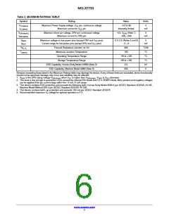
NCL37733
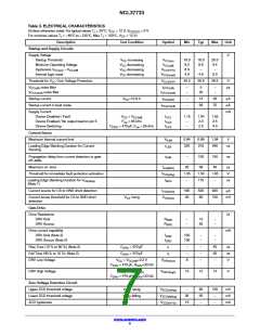
Constant Current Control
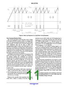
V and V of Figure 4). This circuitry generates the current
S
CS
The NCL37733 embeds an analog/digital block to control
the power factor and regulate the output current by
setpoint (V
) and compares it to the current sense
CONTROL
signal (V ) to dictate the MOSFET turning off event when
CS
monitoring the ZCD, V and CS pin voltages (signals ZCD,
V
CS
exceeds V
.
S
CONTROL
V
VS
V
REFX
ZCD
STOP
PWM Latch reset
V
CS
Power Factor and
Constant−Current
Control
COMP
C1
Figure 4. Power Factor and Constant−Current Control
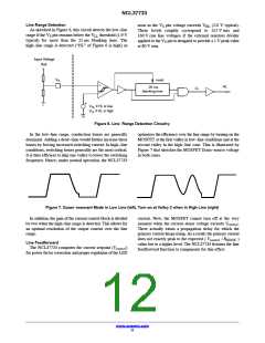
Start−up Sequence
As illustrated in Figure 4, the V pin provides the
S
Generally an LED lamp is expected to emit light in < 1 s
and typically within 500 ms. The start−up phase consists of
sinusoidal reference necessary for shaping the input current.
The obtained current reference is further modulated so that
when averaged over a half−line period, it is equal to the
the time to charge the V capacitor, to begin switching and
CC
the time to charge the output capacitor until sufficient
current flows into the LED string. To speed−up this phase,
the following characteristics define the start−up sequence:
output current reference (V
). This averaging process is
REFX
made by an internal Operational Trans−conductance
Amplifier (OTA) and the capacitor connected to the COMP
pin (C1 of Figure 4). Typical COMP capacitance is 1 mF and
should not be less than 470 nF to ensure stability. The COMP
ripple does not affect the power factor performance as the
circuit digitally eliminates it when generating the current
setpoint.
• The COMP pin is grounded when the circuit is off. The
average COMP voltage needs to exceed the V pin
S
peak value to have the LED current properly regulated
(whatever the current target is). To speed−up the COMP
capacitance charge and shorten the start−up phase, an
internal 80 mA current source adds to the OTA sourced
current (60 mA max typically) to charge up the COMP
capacitance. The 80 mA current source remains on until
the OTA starts to sink current as a result of the COMP
pin voltage sufficient rise. At that moment, the COMP
pin being near its steady−state value, only the OTA
drives the COMP pin.
If the V pin properly conveys the sinusoidal shape, power
S
factor will be close to unity and the Total Harmonic
Distortion (THD) will be low. In any case, the output current
will be well regulated following the equation below:
VREF
2 NPS Rsense
Iout
+
(eq. 1)
Where:
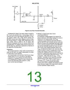
• If the load is shorted, the circuit will operate in hiccup
• N is the secondary to primary transformer turns
PS
mode with V oscillating between V
and
CC
CC(off)
N
• R
• V
= N / N
S P
PS
V
CC(on)
until the Auxiliary Short Circuit Protection,
is the current sense resistor (see Figure 1).
sense
REF
AUX_SCP, forces the 4 s auto−recovery delay to reduce
the operation duty−ratio (AUX_SCP trips if the ZCD
pin voltage does not exceed 1 V within a 90 ms active
period of time thus indicating a short to ground of the
ZCD pin or an excessive load preventing the output
voltage from rising). Figure 5 illustrates a start−up
sequence with the output shorted to ground.
is the output current internal reference (200 mV).
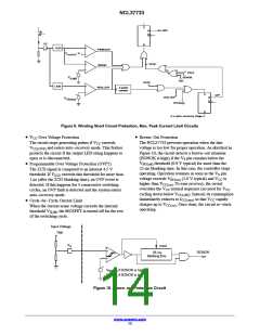
Whenever a major fault is detected which forces the
auto−recovery mode, the COMP pin is grounded for the 4−s
interruption. This is also the case if one of these situations
is detected: brown−out, UVLO, TSD fault. This ensures a
clean start−up when the circuit resumes operation.
www.onsemi.com
9

 ONSEMI [ ONSEMI ]