NCL37733
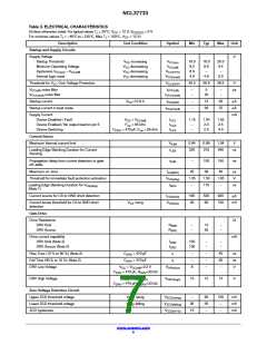
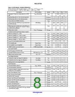
Table 3. ELECTRICAL CHARACTERISTICS
(Unless otherwise noted: For typical values T = 25°C, V = 12 V, V = 0 V
J
CC
CS/ZCD
For min/max values T = −40°C to +125°C, Max T = 150°C, V = 12 V)
J
J
CC
Description
Test Condition
decreasing
Symbol
Min
Typ
Max
Unit
Propagation Delay from valley detection to DRV
high
V
t
−
200
300
ns
ZCD
DEM
Blanking delay after on−time (normal operation)
Blanking delay after on−time (startup phase)
Timeout after last DEMAG transition
t
t
1.12
2.24
6.0
1.50
3.00
7.3
1.88
3.76
9.0
ms
ms
ms
ns
ZCD(blank1)
ZCD(blank2)
t
t
TIMO
Time for which the CS/ZCD pin is grounded when
the DRV turns low
DRV falling
T
1
200
325
450
Watch Dog Timer (restart timer in the absence of
demagnetization signal like for instance in startup
or short circuit conditions)
40
55
70
ms
WDG
Pulling−down resistor
V
ZCD
= V
R
ZCD(pd)
200
kW
ZCD(falling)
Constant Current and Power Factor Control
Reference Voltage at T = 25°C
V
V
V
V
195
192.5
190
187.5
−
200
200.0
200
200.0
4
205
207.5
210
212.5
−
mV
mV
mV
mV
−
j
REF
REF
REF
REF
Reference Voltage at T = 25°C to 100°C
j
Reference Voltage at T = −20°C to 125°C
j
Reference Voltage T = −40°C to 125°C
j
V
control
to current setpoint division ratio
V
ratio
Error amplifier gain
V
V
=V
=V
G
44
54
64
mS
mA
mA
REFX
REF
EA
Error amplifier current capability
COMP Pin Start−up Current Source
Line Feed Forward
I
EA
60
REFX
REF
COMP pin grounded
I
125
EA_STUP
V
to I
conversion ratio
K
9.8
19.5
44
10.9
22.0
53
11.8
24.5
64
mS
mA
mA
VS
CS(offset)
LFF
Line feed−forward current on CS pin
Offset current maximum value
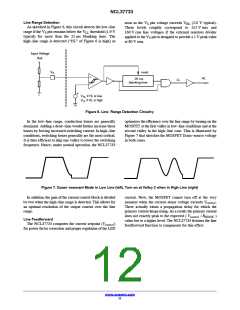
Line Range Detection
DRV high, V = 2 V
I
VS
LFF
V
VS
> 5 V
I
offset(MAX)
Threshold for high−line range (HL) detection
Threshold for low−line range (LL) detection
Blanking time for line range detection
Fault Protection
V
rising
falling
V
1.9
1.8
15
2.0
1.9
25
2.1
2.0
35
V
V
VS
VS
HL
V
V
LL
HL(blank)
t
ms
Thermal Shutdown (Note 2)
F
SW
= 65 kHz
T
130
−
150
50
170
−
°C
°C
V
SHDN
T
SHDN(HYS)
Thermal Shutdown Hysteresis
Threshold voltage for output short circuit or aux.
winding short circuit detection
V
0.94
0.99
1.04
ZCD(short)
Short circuit detection Timer
Auto−recovery timer duration
CS/ZCD OVP Threshold
V
< V
t
OVLD
70
3
90
4
110
5
ms
s
ZCD
ZCD(short)
t
recovery
V
4.32
0.95
0.85
4.50
1.00
0.90
30
4.68
1.05
0.95
V
OVP2
BO(on)
BO(off)
Brown−Out ON level (IC start pulsing)
Brown−Out OFF level (IC shuts down)
BO comparators delay
V
rising
falling
V
V
V
S
V
S
V
t
ms
ms
nA
BO(delay)
BO(blank)
Brown−Out blanking time
t
15
50
25
35
V
S
pin Pulling−down Current
V
S
= V
I
BO(bias)
250
450
BO(on)
1. The CS/ZCD pin is grounded for the t
2. Guaranteed by Design
duration
BCS
www.onsemi.com
7

 ONSEMI [ ONSEMI ]