NCL37733
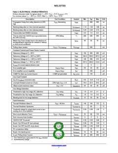
Table 3. ELECTRICAL CHARACTERISTICS
(Unless otherwise noted: For typical values T = 25°C, V = 12 V, V = 0 V
J
CC
CS/ZCD
For min/max values T = −40°C to +125°C, Max T = 150°C, V = 12 V)
J
J
CC
Description
Test Condition
Symbol
Min
Typ
Max
Unit
Startup and Supply Circuits
Supply Voltage
V
Startup Threshold
Minimum Operating Voltage
V
increasing
decreasing
decreasing
decreasing
V
V
16.0
8.2
8.0
4.0
18.0
8.8
−
20.0
9.4
−
CC
CC(on)
V
CC
V
CC
V
CC
CC(off)
Hysteresis V
– V
V
CC(on)
CC(off)
CC(HYS)
CC(reset)
Internal logic reset
V
4.8
6.0
Threshold for V Over Voltage Protection
V
25.5
26.8
28.5
V
CC
CC(OVP)
V
V
noise filter
t
−
−
5
20
−
−
ms
CC(off)
VCC(off)
noise filter
t
CC(reset)
VCC(reset)
Startup current
V
CC
=15.9 V
I
−
−
13
58
30
75
mA
mA
CC(start)
Startup current in fault mode
I
CC(sFault)
Supply Current
mA
Device Disabled / Fault
Device Enabled / No output load on pin 5
Device Switching
V
F
> V
= 65 kHz
I
I
I
1.15
–
−
1.34
2.0
2.5
1.55
3.5
4.0
CC
CC(off)
CC1
CC2
CC3
sw
C
= 470 pF, F = 65 kHz
DRV
sw
Current Sense
Maximum Internal current limit
V
0.94
220
0.99
275
1.04
340
V
ILIM
Leading Edge Blanking Duration for Current
Sensing
t
ns
LEB
Propagation delay from current detection to gate
off−state
t
−
100
150
ns
ILIM
Maximum on−time
t
26
1.35
−
36
46
1.65
−
ms
V
on(MAX)
Threshold for immediate fault protection activation
V
1.50
175
CS(stop)
Leading Edge Blanking Duration for V
(Note 1)
t
ns
CS(stop)
BCS
Current source for CS to GND short detection
I
420
30
520
90
620
150
mA
CS(short)
Current sense threshold for CS to GND short
detection
V
CS
rising
V
mV
CS(low)
Gate Drive
Drive Resistance
DRV Sink
W
R
R
−
−
13
30
−
−
SNK
DRV Source
SRC
Drive current capability
DRV Sink (Note 2)
mA
I
150
100
−
−
−
−
SNK
DRV Source (Note 2)
I
SRC
Rise Time (10 % to 90 %) (Note 2)
Fall Time (90 % to 10 %) (Note 2)
DRV Low Voltage
C
C
= 470 pF
= 470 pF
t
–
–
8
−
−
–
45
35
−
ns
ns
V
DRV
r
t
DRV
f
V
= V
+0.2 V
CC(off)
V
CC
DRV(low)
C
C
= 470 pF, R
=33 kW
DRV
DRV
DRV High Voltage
V
CC
= V
V
10
12
14
V
CC(MAX)
DRV(high)
= 470 pF, R
=33 kW
DRV
DRV
Zero Voltage Detection Circuit
Upper ZCD threshold voltage
Lower ZCD threshold voltage
ZCD hysteresis
V
rising
V
−
90
55
−
150
−
mV
mV
mV
ZCD
ZCD(rising)
V
ZCD
falling
V
35
15
ZCD(falling)
V
−
ZCD(HYS)
www.onsemi.com
6

 ONSEMI [ ONSEMI ]