NCL37733
Input Voltage
Rail
V
S
V
DD
CS/ZCD
R
I
CS
LFF
R
SENSE
DRV
NCL37733
.
Auxiliary
winding
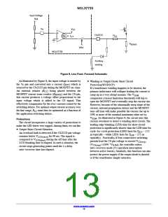
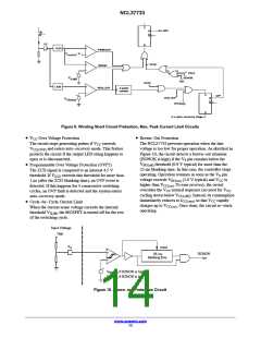
Figure 8. Line Feed−Forward Schematic
As illustrated by Figure 8, the input voltage is sensed by
the V pin and converted into a current (I ) which is
• Winding or Output Diode Short Circuit
Protection(WODSCP)
S
LFF
sourced by the CS/ZCD pin during the MOSFET on−time.
An external resistor (R ) being placed between the
If a transformer winding happens to be shorted, the
primary inductance will collapse leading the current to
ramp up in a very abrupt manner. The V
CS
MOSFET current sense resistor (R
) and the CS pin,
SENSE
ILIM
this current produces a voltage offset proportional to the
input voltage which is added to the CS signal. This
effectively compensates for the over−currents caused by the
switching delays. For optimal output current accuracy over
comparator (current limitation threshold) will trip to
open the MOSFET and eventually stop the current rise.
However, because of the abnormally steep slope of the
current, internal propagation delays and the MOSFET
turn−off time will make possible the current rise up to
50% or more of the nominal maximum value set by
the line range, R must thus be optimized as a function of
CS
the application switching delays.
V
. As illustrated in Figure 9, the circuit uses this
ILIM
Protections
current overshoot to detect a winding short circuit. The
leading edge blanking (LEB) time for short circuit
protection is significantly shorter than the LEB time for
cycle−by−cycle protection (LEB2 lasts for T
ns typically – while LEB1 lasts for T
typically). Practically, if four consecutive switching
periods lead the CS pin voltage to exceed V
(V
auto−recovery mode (4 s operation interruption
between active bursts). Similarly, this function can also
protect the power supply if the output diode is shorted
or if the transformer simply saturates.
The circuit incorporates a large variety of protections to
make the LED driver very rugged. Among them, we can list:
• Output Short Circuit Situation
– 175
BCS
An overload fault is detected if the CS/ZCD pin voltage
– 275 ns
LEB
remains below V
compared to V
ZCD blanking time is elapsed. In such a situation, the
circuit stops generating pulses until the 4 s delay
auto−recovery time has elapsed.
for 90 ms. The signal is
during the off time after the
ZCD(short)
ZCD(short)
CS(stop)
=150% *V ), the controller enters
CS(stop) ILIM
www.onsemi.com
12

 ONSEMI [ ONSEMI ]