NCL37733
APPLICATION INFORMATION
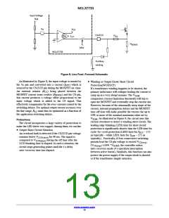
The NCL37733 is designed to control flyback−,
switching cycles, the controller stops operating for
the 4−s auto−recovery delay.
♦ Cycle−by−cycle peak current limit:
buck−boost− and SEPIC−based LED drivers. A proprietary
circuitry ensures accurate primary−side regulation of the
output current (without the need for a secondary−side
feedback) and near−unity power factor correction. The
circuit contains a suite of powerful protections to ensure a
robust LED driver design without the need for extra
components or overdesign.
when the current sense voltage exceeds the internal
threshold V , the MOSFET is immediately
ILIM
turned off (cycle by cycle current limitation).
♦ Winding or Output Diode Short−Circuit Protection
(WODSCP):
an additional comparator senses the CS signal and
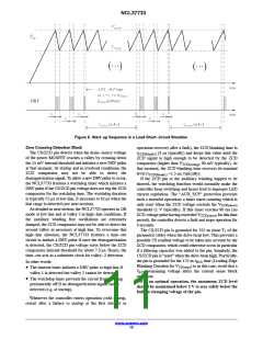
• Quasi−Resonance Current−Mode Operation:
implementing quasi−resonance operation in peak
current−mode control, the NCL37733 optimizes the
efficiency by switching in the valley of the MOSFET
drain−source voltage in low−line conditions. When in
high line, the circuit skips one valley to lower the
switching frequency.
stops the controller if it exceeds 150% x V
for 4
ILIM
consecutive cycles. This feature can protect the
converter if a winding is shorted or if the output
diode is shorted or simply if the transformer
saturates.
♦ Auxiliary Short−circuit protection (AUX_SCP):
If the ZCD pin voltage remains low for a 90 ms time
interval, the controller detects that the output or the
ZCD pin is grounded and hence, stops pulsating
until a 4 s time has elapsed.
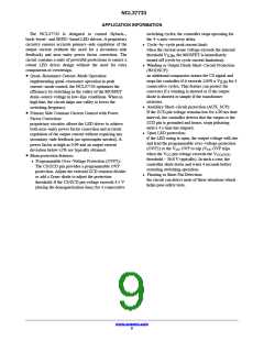
• Primary Side Constant Current Control with Power
Factor Correction:
proprietary circuitry allows the LED driver to achieve
both near−unity power factor correction and accurate
regulation of the output current without requiring any
secondary−side feedback (no optocoupler needed). A
power factor as high as 0.99 and an output current
deviation below 2% are typically obtained.
♦ Open LED protection:
if the LED string is open, the output voltage will rise
and lead the programmable over−voltage protection
(OVP2) or the V OVP to trip (V OVP trips
CC
CC
when the V pin voltage exceeds the V
CC
CC(OVP)
• Main protection features:
threshold – 26.8 V typically). In such a case, the
controller shuts down and waits 4 seconds before
restarting switching operation.
♦ Programmable Over−Voltage Protection (OVP2):
The CS/ZCD pin provides a programmable OVP
protection. Adjust the external ZCD resistors divider
or add a Zener diode to adjust the protection
threshold: if the CS/ZCD pin voltage exceeds 4.5 V
(during the demagnetization time) for 4 consecutive
♦ Floating or Short Pin Detection:
the circuit can detect most of these situations which
helps pass safety tests.
www.onsemi.com
8

 ONSEMI [ ONSEMI ]