NCL37733
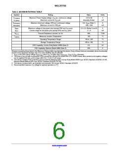
Table 2. MAXIMUM RATINGS TABLE
Symbol
Rating
Value
Units
V
Maximum Power Supply voltage, V pin, continuous voltage
−0.3 to 30
V
CC(MAX)
CC
I
Maximum current for V pin
Internally limited
mA
CC(MAX)
CC
V
Maximum driver pin voltage, DRV pin, continuous voltage
Maximum current for DRV pin
−0.3, V
(Note 1)
V
mA
DRV(MAX)
DRV
I
−300, +500
DRV(MAX)
V
Maximum voltage on low power pins (except DRV and V pins)
−0.3, 5.5 (Notes 2 and 5)
−2, +5
V
mA
MAX
CC
I
Current range for low power pins (except DRV and V pins)
MAX
CC
R
Thermal Resistance Junction−to−Air
Maximum Junction Temperature
360
150
°C/W
°C
θ
J−A
T
J(MAX)
Operating Temperature Range
−40 to +125
−60 to +150
3.5
°C
Storage Temperature Range
°C
ESD Capability, Human Body Model (HBM) (Note 3)
ESD Capability, Machine Model (MM) (Note 3)
kV
V
250
Stresses exceeding those listed in the Maximum Ratings table may damage the device. If any of these limits are exceeded, device functionality
should not be assumed, damage may occur and reliability may be affected.
1. V
is the DRV clamp voltage V
when V is higher than V
. V
is V otherwise.
DRV
DRV(high)
CC
DRV(high) DRV CC
2. This level is low enough to guarantee not to exceed the internal ESD diode and 5.5 V ZENER diode. More positive and negative voltages
can be applied if the pin current stays within the −2 mA / 5 mA range.
3. This device contains ESD protection and exceeds the following tests: Human Body Model 3500 V per JEDEC Standard JESD22−A114E,
Machine Model Method 250 V per JEDEC Standard JESD22−A115B.
4. This device contains latch−up protection and exceeds 100 mA per JEDEC Standard JESD78.
5. Recommended maximum V voltage for optimal operation is 4 V.
S
www.onsemi.com
5

 ONSEMI [ ONSEMI ]