NCL30486B
Dimming Standby Mode (dimCV Mode)
• R
is the resistor connected between ZCD and GND
is the auxiliary winding voltage corresponding to
ZCDL
pins
The NCL30486B features an option to force constant
voltage regulation by pulling ADIM or PDIM pin down.
This can be useful to provide some energy to secondary side
circuitry while the LED are turned off. In this mode, the
regulation target is set lower than the regulation threshold is
normal CV mode.
• V
auxCV1
the nominal CV setpoint
• V
is the auxiliary winding voltage corresponding to
auxCV2
the CV setpoint in reduced CV mode: V
< V
auxCV2
auxCV1
Concretely, when V
internal PDIM signal on−time is below 10 ms during 20 ms,
the “dimCVmode” signal becomes high and the I
current source is applied to ZCD pin during the
demagnetization time only (this is to allow correct valley
detection). This current sources increases ZCD voltage and
consequently a new regulation point is set for the CV loop.
The ZCD pin resistors set directly the regulation threshold
in normal CV mode and in dimming CV mode.
< V
or when the
ADIM
ADIM(EN)
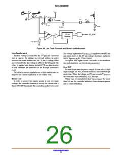
Valley Lockout
Quasi−Square wave resonant systems have a wide
switching frequency excursion. The switching frequency
increases when the output load decreases or when the input
voltage increases. The switching frequency of such systems
must be limited.
ZCD(dim)
The NCL30486B changes valley as V
decreases and
REFX
as the input voltage increases and as the output current
setpoint is varied during dimming. This limits the frequency
excursion.
By default, when the output current is not dimmed, the
controller operates in the first valley at low line and in the
second valley at high line.
There is an option to have the valley thresholds
incremented by 1 at high line for better I control at
305 V rms.
V
REF(CV) (VauxCV1 * VauxCV2)
(eq. 2)
RZCDL
+
I
ZCD(dim) (VauxCV1 * VREF(CV))
VauxCV1
ǒ Ǔ
(eq. 3)
RZCDU + RZCDL
* 1
VREF(CV)
out
Where:
• R
is the resistor from auxiliary winding to ZCD pin
ZCDU
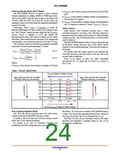
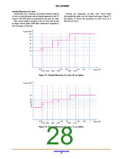
Table 1. VALLEY SELECTION
V
Voltage for Valley Change
HV_DIV
V
REFX
Value at which the Controller
V
REFX
Value at which the Controller
0
−−LL−−
2.3 V
−−HL−−
5 V
Changes Valley (I
Decreasing)
Changes Valley (I
Increasing)
out
out
st
nd rd
100%
100%
1
2
3
4
5
6
(3 )
90%
75%
60%
45%
80%
65%
50%
35%
nd
rd th
2
(4 )
rd
th th
3
(5 )
th
th th
4
(6 )
th
th th
5
(7 )
25%
0%
35%
0%
FF mode
FF mode
0
−−LL−−
2.3 V
−−HL−−
5 V
Internal V
Voltage for Valley Change
HV_DIV
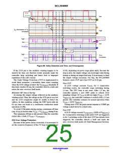
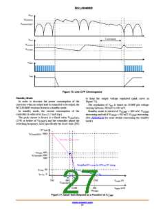
Zero Crossing Detection Block
the valleys. To avoid such a situation, NCL30486B features
a Time−Out circuit that generates pulses if the voltage on
ZCD pin stays below the 55 mV threshold for 6.5 ms.
The Time−out also acts as a substitute clock for the valley
detection and simulates a missing valley in case of too
damped free oscillations.
The ZCD pin allows detecting when the drain−source
voltage of the power MOSFET reaches a valley.
A valley is detected when the ZCD pin voltage crosses
below the 55 mV internal threshold.
At startup or in case of extremely damped free
oscillations, the ZCD comparator may not be able to detect
www.onsemi.com
24

 ONSEMI [ ONSEMI ]