NCL30486B
The output current reference (V
) is V
unless the
The sampled voltage is applied to the negative input of the
constant voltage (CV) operational transconductance
REFX
REF
constant voltage mode is activated or ADIM pin voltage is
below V or a PWM signal with a duty−cycle below
amplifier (OTA) and compared to V
.
ADIM(100)
REFCV
95% is applied on PDIM.
A type 2 compensator is needed at the CV OTA output to
stabilize the loop. The COMP pin voltage modify the the
output current internal reference in order to regulate the
output voltage.
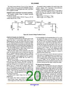
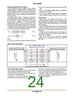
PRIMARY SIDE CONSTANT VOLTAGE CONTROL
The auxiliary winding voltage is sampled internally
through the ZCD pin.
A precise internal voltage reference V
voltage target for the CV loop.
When V
When V
≥ 4 V, V
= V
.
COMP
COMP
REFX
< 0.9 V, V
REF
sets the
REF(CV)
= 0 V.
REFX
Gm
RZCDU
ZCD
V
ZCDsamp
ZCD & signal
sampling
COMP
.
R1
C1
R
OTA
ZCDL
VREF(CV)
C2
Aux.
Figure 62. Constant Voltage Feedback Circuit
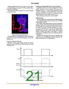
STARTUP PHASE (HV STARTUP)
• At the beginning of each operating phase of a V cycle,
CC
It is generally requested that the LED driver starts to emit
light in less than 1 s and possibly within 300 ms. It is
challenging since the start−up consists of the time to charge
the digital OTA output is set to 0. Actually, the digital
OTA output is set to 0 in the case of a cold start−up or in
the case of a start−up sequence following an operation
the V capacitor and that necessary to charge the output
CC
interruption due to a fault. On the other hand, if the V
CC
capacitor until sufficient current flows into the LED string.
This second phase can be particularly long in dimming cases
where the secondary current is a portion of the nominal one.
The NCL30486B features a high voltage startup circuit
that allows charging VCC capacitor very fast.
hiccups just because the system fails to start−up in one
cycle, the digital OTA output is not reset to ease the
V
CC
second (or more) attempt. But, the digital OTA stops
integrating if V < V . The compensator output
CC
CC(off)
then restarts from its setpoint before the UVLO, thus
avoiding any output current overshoot if a resistor is
inserted in series with HV pin.
When the power supply is first connected to the mains
outlet, the internal current source is biased and charges up
the V capacitor. When the voltage on this V capacitor
CC
CC
• If the load is shorted, the circuit will operate in hiccup
reaches the V
level, the current source turns off. At this
CC(on)
mode with VCC oscillating between V
and V
CC(on)
CC(off)
time, the controller is only supplied by the V capacitor,
CC
until the output under voltage protection (UVP) trips.
UVP is triggered if the ZCD pin voltage does not exceed
and the auxiliary supply should take over before V
CC
collapses below V
.
CC(off)
V
within a 90 ms operation of time. This
ZCD(short)
The HV startup circuitry is made of two startup current
levels, I and I . This helps to protect the
indicates that the ZCD pin is shorted to ground or that an
excessive load prevents the output voltage from rising.
HV(start1)
HV(start2)
controller against short−circuit between V and GND. At
CC
power−up, as long as V is below V
, the source
CC
CC(TH)
HV Startup Power Dissipation
delivers I
(around 300 mA typical). Then, when
HV(start1)
At high line (305 V rms and above) the power dissipated
by the HV startup in case of fault or when the controller is
disabled with PDIM becomes high. Indeed, in case of fault,
the NCL30486B is directly supplied by the HV rail. When
the controller is disabled with PDIM, the optocoupler
collector current is also supplied by the controller, since the
NCL30486B allows directly connecting the optocoupler
transistor to PDIM pin. Thus, the HV startup circuit also
supplies the optocoupler transistor in case of faults. The
current flowing through the HV startup will heat the
controller. It is highly recommended adding enough copper
V
reaches V
, the source smoothly transitions to
CC
CC(TH)
I
and delivers its nominal value. As a result, in case
HV(start2)
of short−circuit between V and GND occurring at high
line (V = 305 V rms), the maximum power dissipation will
be 431 x 300 m = 130 mW instead of 1.5 W if there was only
one startup current level.
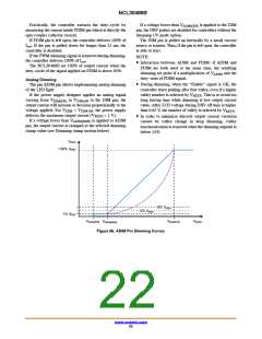
To speed−up the output voltage rise, the following is
implemented:
CC
in
• The digital OTA output is increased until V
REF(PFC)
signal reaches V
. Again, this is to speed−up the
REFX
control signal rise to their steady state value.
around the controller to decrease the R
of the controller.
qJA
www.onsemi.com
20

 ONSEMI [ ONSEMI ]