MT9M021, MT9M031
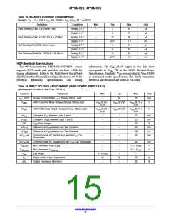
Table 15. STANDBY CURRENT CONSUMPTION
(Analog − V + V _PIX + V _PLL; Digital − V + V _IO; T = 25°C)
AA
AA
DD
DD
DD
A
Definition
Condition
Analog, 2.8 V
Digital, 1.8 V
Analog, 2.8 V
Digital, 1.8 V
Analog, 2.8 V
Digital, 1.8 V
Analog, 2.8 V
Digital, 1.8 V
Min
–
Typ
3
Max
10
Unit
mA
Hard Standby (Clock Off, Driven Low)
Hard Standby (Clock On, EXTCLK = 20 MHz)
Soft Standby (Clock Off, Driven Low)
–
8
75
mA
–
12
0.87
3
20
mA
–
1.3
10
mA
mA
–
–
8
75
mA
Soft Standby (Clock On, EXTCLK = 20 MHz)
–
12
0.87
20
mA
–
1.3
mA
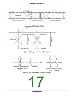
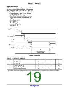
HiSPi Electrical Specifications
The ON Semiconductor MT9M021/MT9M031 sensor
supports SLVS mode only, and does not have a DLL for
timing adjustments. Refer to the High-Speed Serial Pixel
(HiSPi) Interface Physical Layer Specification v2.00.00 for
electrical definitions, specifications, and timing
information. The V _SLVS supply in this data sheet
DD
corresponds to V _TX in the HiSPi Physical Layer
DD
Specification. Similarly, V is equivalent to V _HiSPi
DD
DD
as referenced in the specification. The HiSPi transmitter
electrical specifications are listed at 700 MHz.
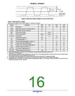
Table 16. INPUT VOLTAGE AND CURRENT (HiSPi POWER SUPPLY 0.4 V)
(Measurement Conditions: Max Freq. 700 MHz)
Symbol
_SLVS
Parameter
) (Driving 100 W Load)
HiSPi
Min
Typ
Max
Unit
mA
V
I
Supply Current (PWR
–
10
15
DD
V
CMD
HiSPi Common Mode Voltage (Driving 100 W Load)
V
_SLVS x
0.45
V
V
_SLVS/2
V
V
_SLVS x
DD
0.55
DD
DD
|V
|
HiSPi Differential Output Voltage (Driving 100 W Load)
V
_SLVS x
0.36
_SLVS/2
_SLVS x
DD
0.64
V
OD
DD
DD
DV
Change in V
between Logic 1 and 0
−
−
–
−
−
−
−
−
−
−
−
−
25
25
mV
mV
%
CM
CM
|V
|
Change in |V | between Logic 1 and 0
OD
OD
NM
V
OD
Noise Margin
30
|DV
|DV
|
Difference in V
between any Two Channels
50
mV
mV
mV
CM
CM
|
Difference in V between any Two Channels
100
50
OD
OD
DV _ac
Common-mode AC Voltage (pk) without V
Cap
CM
CM
Termination
DV _ac
Common-mode AC Voltage (pk) with V
Cap Termination
−
−
−
−
−
30
mV
V
CM
CM
V
OD
_ac
Max Overshoot Peak |V
|
1.3 x |V
2.6 x |V
−
|
|
OD
diff pk-pk
OD
V
Max Overshoot V
Eye Height
−
V
diff_pkpk
OD
V
eye
1.4 x V
−
OD
R
Single-ended Output Impedance
Output Impedance Mismatch
35
−
50
−
70
W
o
DR
20
%
o
www.onsemi.com
15

 ONSEMI [ ONSEMI ]