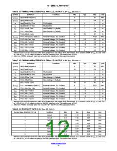
MT9M021, MT9M031
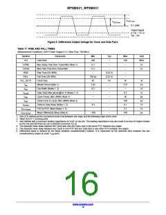
V
DIFFmax
V
DIFFmin
0 V (Diff)
Output Signal
is ‘Cp − Cn’ or
‘Dp − Dn’
Figure 8. Differential Output Voltage for Clock and Data Pairs
Table 17. RISE AND FALL TIMES
(Measurement Conditions: HiSPi Power Supply 0.4 V, Max Freq. 700 MHz)
Symbol
1/UI
Parameter
Min
280
0.3
0.3
–
Typ
Max
700
–
Unit
Mb/s
UI
Data Rate
–
TxPRE
TxPost
RISE
Max Setup Time from Transmitter (Note 1)
Max Hold Time from Transmitter
Rise Time (20−80%)
–
–
–
UI
0.25 UI
–
FALL
Fall Time (20−80%)
150 ps
45
0.25 UI
–
PLL_DUTY
Clock Duty
50
−
55
3.57
−
%
ns
UI
UI
ps
ps
UI
UI
ps
t
pw
Bitrate Period (Note 1)
1.43
0.3
−
t
Eye Width (Notes 1, 2)
−
eye
t
Data Total Jitter (pk pk)@1e−9 (Notes 1, 2)
Clock Period Jitter (RMS) (Note 2)
Clock Cycle to Cycle Jitter (RMS) (Note 2)
Clock to Data Skew (Notes 1, 2)
PHY-to-PHY Skew (Notes 1, 5)
Mean Differential Skew (Note 6)
−
0.2
50
100
0.1
2.1
100
totaljit
t
t
−
−
ckjit
−
−
cyjit
t
−0.1
−
−
chskew
t
−
|PHYskew|
t
–100
−
DIFFSKEW
1. One UI is defined as the normalized mean time between one edge and the following edge of the clock.
2. Taken from 0 V crossing point.
3. Also defined with a maximum loading capacitance of 10 pF on any pin. The loading capacitance may also need to be less for higher bitrates
so the rise and fall times do not exceed the maximum 0.3 UI.
4. The absolute mean skew between the Clock lane and any Data Lane in the same PHY between any edges.
5. The absolute mean skew between any Clock in one PHY and any Data lane in any other PHY between any edges.
6. Differential skew is defined as the skew between complementary outputs. It is measured as the absolute time between the two
complementary edges at mean V
point.
CM
www.onsemi.com
16

 ONSEMI [ ONSEMI ]