MT9M021, MT9M031
DC Electrical Characteristics
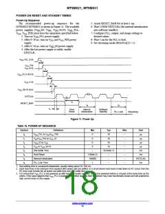
The DC electrical characteristics are shown in Table 12,
Table 13, Table 14, and Table 15.
Table 12. DC ELECTRICAL CHARACTERISTICS
Symbol
Definition
Core Digital Voltage
I/O Digital Voltage
Analog Voltage
Condition
Min
1.7
Typ
1.8
1.8/2.8
2.8
2.8
2.8
0.4
–
Max
1.95
1.9/3.1
3.1
Unit
V
V
DD
V
DD
_IO
1.7/2.5
2.5
V
V
AA
V
V
_PIX
_PLL
Pixel Supply Voltage
PLL Supply Voltage
HiSPi Supply Voltage
Input HIGH Voltage
Input LOW Voltage
Input Leakage Current
2.5
3.1
V
AA
V
DD
2.5
3.1
V
V
DD
_SLVS
0.3
0.6
V
V
IH
V
DD
_IO * 0.7
–
V
V
IL
–
–
V
_IO * 0.3
–
V
DD
I
IN
No Pull-up Resistor;
20
–
mA
V
IN
= V _IO or D
DD GND
V
Output HIGH Voltage
Output LOW Voltage
Output HIGH Current
Output LOW Current
V
DD
_IO – 0.3
–
–
–
–
–
0.4
–
V
V
OH
V
V
_IO = 2.8 V
–
–22
–
OL
DD
I
At Specified V
At Specified V
mA
mA
OH
OH
OL
I
OL
22
CAUTION: Stresses greater than those listed in Table 13 may cause permanent damage to the device. This is a stress rating only, and
functional operation of the device at these or any other conditions above those indicated in the operational sections of this
specification is not implied.
Table 13. ABSOLUTE MAXIMUM RATINGS
Symbol
Parameter
Power Supply Voltage (All Supplies)
Total Power Supply Current
Total Ground Current
Minimum
–0.3
–
Maximum
4.5
Unit
V
V
SUPPLY
SUPPLY
I
200
mA
mA
V
I
–
200
GND
V
IN
DC Input Voltage
–0.3
–0.3
–40
V
V
_IO + 0.3
_IO + 0.3
+85
DD
V
OUT
T
STG
DC Output Voltage
V
DD
Storage Temperature (Note 1)
°C
Stresses exceeding those listed in the Maximum Ratings table may damage the device. If any of these limits are exceeded, device functionality
should not be assumed, damage may occur and reliability may be affected.
1. Exposure to absolute maximum rating conditions for extended periods may affect reliability.
Table 14. OPERATING CURRENT CONSUMPTION FOR PARALLEL OUTPUT
(V = V _PIX = V _IO = V _PLL = 2.8 V; V = 1.8 V; PLL Enabled and PIXCLK = 74.25 MHz; T = 25°C; C = 10 pF)
AA
AA
DD
DD
DD
A
LOAD
Symbol
Parameter
Condition
Min
−
Typ
Max
Unit
mA
mA
I
Digital Operating Current
Parallel, Streaming, Full Resolution 45 fps
Parallel, Streaming, Full Resolution 45 fps
45
55
–
DD
I
_IO
I/O Digital Operating Current
−
50
DD
(Note 1)
I
Analog Operating Current
Pixel Supply Current
PLL Supply Current
Parallel, Streaming, Full Resolution 45 fps
Parallel, Streaming, Full Resolution 45 fps
Parallel, Streaming, Full Resolution 45 fps
−
−
−
45
6
50
10
8
mA
mA
mA
AA
I
_PIX
AA
_PLL
DD
I
6
1. I _IO operating current is specified with image at 1/2 saturation level.
DD
www.onsemi.com
14

 ONSEMI [ ONSEMI ]