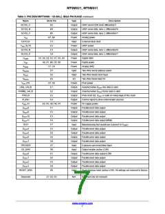
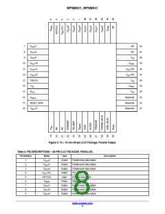
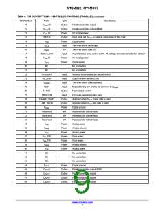
MT9M021, MT9M031
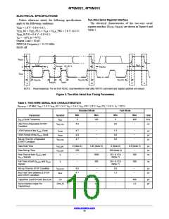
Table 5. TWO-WIRE SERIAL BUS CHARACTERISTICS (continued)
(f
= 27 MHz; V = 1.8 V; V _IO = 2.8 V; V = 2.8 V; V _PIX = 2.8 V; V _PLL = 2.8 V; T = 25°C)
EXTCLK
DD
DD
AA
AA
DD
A
Standard Mode
Fast-Mode
Min
Max
Min
−
Max
30
Parameter
Symbol
CLOAD_SD
RSD
Unit
pF
S
S
Max Load Capacitance
−
30
DATA
Pull-up Resistor
1.5
4.7
1.5
4.7
kW
DATA
2
1. This table is based on I C standard (v2.1 January 2000). Philips Semiconductor.
2
2. Two-wire control is I C-compatible.
3. All values referred to V
= 0.9 V _IO and V
= 0.1 V _IO levels. Sensor EXCLK = 27 MHz.
ILmax DD
IHmin
DD
4. A device must internally provide a hold time of at least 300 ns for the S
signal to bridge the undefined region of the falling edge of S
.
DATA
CLK
5. The maximum t
has only to be met if the device does not stretch the LOW period (t
) of the S
signal.
HD;DAT
LOW
CLK
2
2
6. A Fast-mode I C-bus device can be used in a Standard-mode I C-bus system, but the requirement t
250 ns must then be met. This
SU;DAT
will automatically be the case if the device does not stretch the LOW period of the S
signal. If such a device does stretch the LOW period
CLK
of the S
signal, it must output the next data bit to the S
line t max + t
= 1000 + 250 = 1250 ns (according to the Standard-mode
CLK
DATA
r
SU;DAT
2
I C-bus specification) before the S
line is released.
CLK
7. Cb = total capacitance of one bus line in pF.
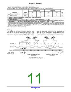
I/O Timing
By default, the MT9M021/MT9M031 launches pixel
data, FV and LV with the falling edge of PIXCLK. The
using the rising edge of PIXCLK. The launch edge of
PIXCLK can be configured in register R0x3028. See
Figure 7 and Table 6 for I/O timing (AC) characteristics.
expectation is that the user captures D [11:0], FV and LV
OUT
t
t
t
t
FP
R
F
RP
90%
10%
90%
10%
90%
10%
90%
10%
t
EXTCLK
EXTCLK
PIXCLK
t
PD
Pxl_0
Pxl_1
Pxl_2
Pxl_n
Data[11:0]
t
t
PFL
t
t
PLH
PFH
LINE_VALID/
PLL
FRAME_VALID
FRAME_VALID Leads LINE_VALID
by 6 PIXCLKs
FRAME_VALID Trails LINE_VALID
by 6 PIXCLKs
Figure 7. I/O Timing Diagram
www.onsemi.com
11

 ONSEMI [ ONSEMI ]