MT9M021, MT9M031
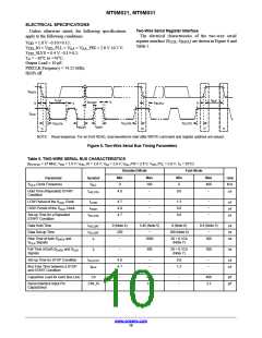
Table 6. I/O TIMING CHARACTERISTICS, PARALLEL OUTPUT (1.8 V VDD_IO) (Note 1)
Symbol
Definition
Input Clock Frequency
Input Clock Period
Condition
Min
6
Typ
−
Max
50
Unit
MHz
ns
f
t
EXTCLK
EXTCLK
20
−
−
166
4
t
R
Input Clock Rise Time
Input Clock Fall Time
PIXCLK Rise Time
PLL Enabled
PLL Enabled
3
ns
t
F
−
3
4
ns
t
Slew Setting = 4 (Default)
Slew Setting = 4 (Default)
2.3
3
−
4.6
4.4
60
ns
RP
t
FP
PIXCLK Fall Time
−
ns
PIXCLK Duty Cycle
PIXCLK Frequency (Note 2)
PIXCLK to Data Valid
PIXCLK to FV HIGH
PIXCLK to LV HIGH
PIXCLK to FV LOW
PIXCLK to LV LOW
40
6
50
−
%
f
Nominal Voltages, PLL Enabled
Nominal Voltages, PLL Enabled
Nominal Voltages, PLL Enabled
Nominal Voltages, PLL Enabled
Nominal Voltages, PLL Enabled
Nominal Voltages, PLL Enabled
74.25
4.5
4.5
4.5
4.5
4.5
MHz
ns
PIXCLK
t
−3
−3
−3
−3
−3
2.3
1.5
2.3
1.5
2
PD
t
ns
PFH
t
ns
PLH
t
ns
PFL
t
ns
PLL
1. Minimum and maximum values are taken at the temperature and voltage limits; for instance, 70°C ambient at 90% of V _IO, and −30°C
DD
at 110% of V _IO. All values are taken at the 50% transition point. The loading used is 20 pF.
DD
2. Jitter from PIXCLK is already taken into account in the data for all of the output parameters.
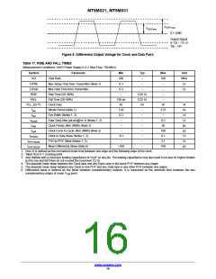
Table 7. I/O TIMING CHARACTERISTICS, PARALLEL OUTPUT (2.8 V VDD_IO) (Note 1)
Symbol
Definition
Condition
Min
Typ
Max
Unit
f
t
Input Clock Frequency
Input Clock Period
6
20
−
−
−
50
166
4
MHz
ns
EXTCLK
EXTCLK
t
R
Input Clock Rise Time
Input Clock Fall Time
PIXCLK Rise Time
PLL Enabled
PLL Enabled
3
ns
t
F
−
3
4
ns
t
Slew Setting = 4 (Default)
Slew Setting = 4 (Default)
2.3
3
−
4.6
4.4
60
74.25
4
ns
RP
t
FP
PIXCLK Fall Time
−
ns
PIXCLK Duty Cycle
PIXCLK Frequency (Note 2)
PIXCLK to Data Valid
PIXCLK to FV HIGH
PIXCLK to LV HIGH
PIXCLK to FV LOW
PIXCLK to LV LOW
40
6
50
−
%
f
Nominal Voltages, PLL Enabled
Nominal Voltages, PLL Enabled
Nominal Voltages, PLL Enabled
Nominal Voltages, PLL Enabled
Nominal Voltages, PLL Enabled
Nominal Voltages, PLL Enabled
MHz
ns
PIXCLK
t
−3
−3
−3
−3
−3
2.3
1.5
2.3
1.5
2
PD
t
4
ns
PFH
t
4
ns
PLH
t
4
ns
PFL
t
4
ns
PLL
1. Minimum and maximum values are taken at the temperature and voltage limits; for instance, 70°C ambient at 90% of V _IO, and −30°C
DD
at 110% of V _IO. All values are taken at the 50% transition point. The loading used is 20 pF.
DD
2. Jitter from PIXCLK is already taken into account in the data for all of the output parameters.
Table 8. I/O RISE SLEW RATE (2.8 V VDD_IO) (Note 1)
Parallel Slew (R0x306E[15:13])
Condition
Min
Typ
Max
Unit
7
6
5
4
3
2
1
0
Default
Default
Default
Default
Default
Default
Default
Default
1.08
0.77
0.58
0.44
0.32
0.23
0.16
0.10
1.77
1.26
0.95
0.70
0.51
0.37
0.25
0.15
2.72
1.94
1.46
1.08
0.78
0.56
0.38
0.22
V/ns
V/ns
V/ns
V/ns
V/ns
V/ns
V/ns
V/ns
1. Minimum and maximum values are taken at the temperature and voltage limits; for instance, 70°C ambient at 90% of V _IO, and −30°C
DD
at 110% of V _IO. All values are taken at the 50% transition point. The loading used is 20 pF.
DD
www.onsemi.com
12

 ONSEMI [ ONSEMI ]