MT9M021, MT9M031
ELECTRICAL SPECIFICATIONS
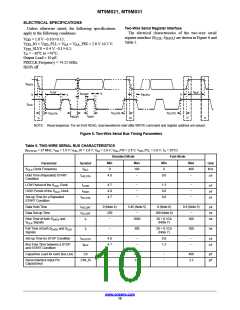
Two-Wire Serial Register Interface
The electrical characteristics of the two-wire serial
Unless otherwise stated, the following specifications
apply to the following conditions:
register interface (S
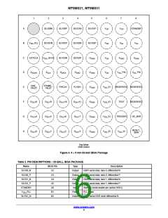
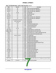
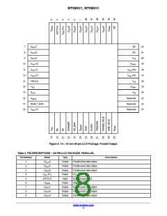
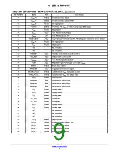
Table 5.
, S
) are shown in Figure 6 and
CLK DATA
V
DD
V
DD
V
DD
= 1.8 V –0.10/+0.15;
_IO = V _PLL = V = V _PIX = 2.8 V 0.3 V;
DD
AA
AA
_SLVS = 0.4 V –0.1/+0.2;
T = −30°C to +70°C;
A
Output Load = 10 pF;
PIXCLK Frequency = 74.25 MHz;
HiSPi off.
S
DATA
t
t
LOW
BUF
t
t
f
SU;DAT
t
t
r
t
f
t
r
HD;STA
S
CLK
t
t
t
SU;STA
SU;STO
HD;STA
t
t
HIGH
HD;DAT
S
Sr
P
S
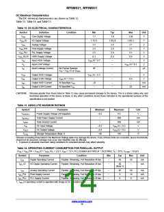
NOTE: Read sequence: For an 8-bit READ, read waveforms start after WRITE command and register address are issued.
Figure 6. Two-Wire Serial Bus Timing Parameters
Table 5. TWO-WIRE SERIAL BUS CHARACTERISTICS
(f
= 27 MHz; V = 1.8 V; V _IO = 2.8 V; V = 2.8 V; V _PIX = 2.8 V; V _PLL = 2.8 V; T = 25°C)
EXTCLK
DD
DD
AA
AA
DD
A
Standard Mode
Fast-Mode
Min
Max
Min
0
Max
400
−
Parameter
Clock Frequency
Symbol
Unit
S
CLK
f
0
100
−
kHz
SCL
Hold Time (Repeated) START
Condition
t
4.0
0.6
ms
HD;STA
LOW Period of the S
Clock
Clock
t
4.7
4.0
4.7
−
−
−
1.3
0.6
0.6
−
−
−
ms
ms
ms
CLK
LOW
HIGH Period of the S
t
HIGH
CLK
Set-up Time for a Repeated
START Condition
t
SU;STA
Data Hold Time
t
0 (Note 4)
3.45 (Note 5)
0 (Note 6)
0.9 (Note 5)
ms
ns
ns
HD;DAT
Data Set-up Time
t
250
−
−
100 (Note 6)
−
SU;DAT
Rise Time of both S
and
t
r
1000
20 + 0.1Cb
(Note 7)
300
DATA
S
CLK
Signals
Fall Time of both S
Signals
and S
t
f
−
300
20 + 0.1Cb
(Note 7)
300
ns
DATA
CLK
Set-up Time for STOP Condition
t
4.0
4.7
−
−
0.6
1.3
−
−
ms
ms
SU;STO
Bus Free Time between a STOP
and START Condition
t
BUF
Capacitive Load for each Bus Line
Cb
−
−
400
3.3
−
−
400
3.3
pF
pF
Serial Interface Input Pin
Capacitance
CIN_SI
www.onsemi.com
10

 ONSEMI [ ONSEMI ]