MT9M021, MT9M031
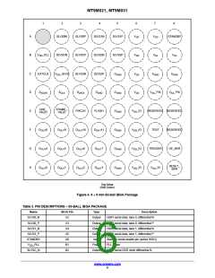
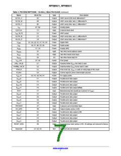
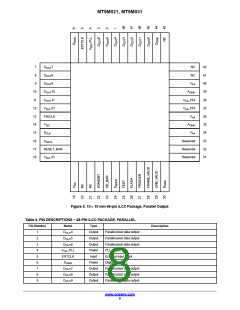
Table 3. PIN DESCRIPTIONS − 63-BALL IBGA PACKAGE (continued)
Name
iBGA Pin
Type
Output
Output
Output
Power
Input
Description
HiSPi serial DDR clock differential P
SLVSC_P
SLVS2_N
SLVS2_P
B3
B4
HiSPi serial data, lane 2, differential N
HiSPi serial data, lane 2, differential P
Analog power
B5
V
AA
B7, B8
EXTCLK
_SLVS
C1
External input clock
V
C2
Power
Output
Output
Power
Power
Power
Input
HiSPi power
DD
SLVS3_N
SLVS3_P
C3
HiSPi serial data, lane 3, differential N
HiSPi serial data, lane 3, differential P
Digital GND
C4
D
C5, D4, D5, E5, F5, G5, H5
GND
V
DD
A6, A7, B6, C6, D6
Digital power
A
GND
C7, C8
Analog GND
S
ADDR
D1
Two-Wire Serial address select
Two-Wire Serial clock input
Two-Wire Serial data I/O
Pixel power
S
CLK
D2
Input
S
DATA
D3
I/O
V
AA
_PIX
D7, D8
Power
Output
Output
Output
Output
Power
Output
Output
Output
Output
Input
LINE_VALID
FRAME_VALID
PIXCLK
E1
Asserted when D
Asserted when D
Pixel clock out. D
line data is valid
OUT
OUT
OUT
E2
frame data is valid
E3
is valid on rising edge of this clock
FLASH
E4
Control signal to drive external light sources
I/O supply power
V
DD
_IO
E6, F6, G6, H6, H7
D
8
OUT
9
OUT
F1
F2
F3
F4
F7
G1
G2
G3
G4
G7
G8
H1
H2
H3
H4
H8
Parallel pixel data output
D
Parallel pixel data output
D
D
10
11
Parallel pixel data output
OUT
Parallel pixel data output (MSB)
Manufacturing test enable pin (connect to D
Parallel pixel data output
OUT
TEST
)
GND
D
4
Output
Output
Output
Output
Input
OUT
OUT
OUT
OUT
D
D
D
5
6
7
Parallel pixel data output
Parallel pixel data output
Parallel pixel data output
TRIGGER
OE_BAR
Exposure synchronization input
Output enable (active LOW)
Parallel pixel data output (LSB)
Parallel pixel data output
Input
D
D
D
D
0
1
2
3
Output
Output
Output
Output
Input
OUT
OUT
OUT
OUT
Parallel pixel data output
Parallel pixel data output
RESET_BAR
Asynchronous reset (active LOW). All settings are restored to factory
default
Reserved
E7, E8, F8
N/A
Reserved (do not connect)
www.onsemi.com
7

 ONSEMI [ ONSEMI ]