ADP3212/NCP3218
1
The compensation values can be calculated as follows:
RSnubber
=
=
(35)
2×π × fRinging ×COSS
n×RO ×TA
RE ×RB
CA
=
=
=
(30)
(31)
1
CSnubber
(36)
TC
CA
π × fRinging × RSnubber
RA
CB
CFB
P
= CSnubber ×VIn2put × fSwithing
(37)
Snubber
TB
RB
(32)
(33)
Where RSnubber is the snubber resistor.
CSnubber is the snubber capacitor.
TD
RA
=
f
Rininging is the frequency of the ringing on the switch node when
the high side MOSFET turns on.
OSS is the low side MOSFET output capacitance at VInput. This is
taken from the low side MOSFET data sheet.
input is the input voltage.
Switching is the switching frequency.
Snubber is the power dissipated in RSnubber
The standard values for these components are subject to the
tuning procedure described in the Tuning Procedure for 12
section.
C
V
f
P
CIN SELECTION AND INPUT CURRENT
di/dt REDUCTION
.
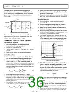
In continuous inductor-current mode, the source current of the
high-side MOSFET is approximately a square wave with a duty
ratio equal to n × VOUT/VIN and an amplitude that is one-nth of
the maximum output current. To prevent large voltage
transients, use a low ESR input capacitor sized for the
maximum rms current. The maximum rms capacitor current
occurs at the lowest input voltage and is given by
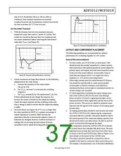
SELECTING THERMAL MONITOR COMPONENTS
To monitor the temperature of a single-point hot spot, set
R
TTSET1 equal to the NTC thermistor’s resistance at the alarm
temperature. For example, if the alarm temperature for VRTT is
100°C and a Vishey thermistor (NTHS-0603N011003J) with a
resistance of 100 kΩ at 25°C, or 6.8 kΩ at 100°C, is used, the
user can set RTTSET1 equal to 6.8 kΩ (the RTH1 at 100°C).
1
ICRMS = D × IO ×
−1
(34)
n× D
1
ICRMS = 0.18 × 40 A ×
−1 = 9.6 A
2 × 0.18
where IO is the output current.
In a typical notebook system, the battery rail decoupling is
achieved by using MLC capacitors or a mixture of MLC
capacitors and bulk capacitors. In this example, the input
capacitor bank is formed by eight pieces of 10 μF, 25 V MLC
capacitors, with a ripple current rating of about 1.5 A each.
Figure 25. Single-Point Thermal Monitoring
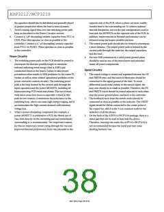
RC SNUBBER
To monitor the temperature of multiple-point hot spots, use the
configuration shown in Figure 26. If any of the monitored hot
spots reaches the alarm temperature, the VRTT signal is
asserted. The following calculation sets the alarm temperature:
It is important in any buck topology to use a resistor-capacitor
snubber across the low side power MOSFET. The RC snubber
dampens ringing on the switch node when the high side
MOSFET turns on. The switch node ringing could cause EMI
system failures and increased stress on the power components
and controller. The RC snubber should be placed as close as
possible to the low side MOSFET. Typical values for the resistor
range from 1 Ω to 10 Ω. Typical values for the capacitor range
from 330 pF to 4.7 nF. The exact value of the RC snubber
depends on the PCB layout and MOSFET selection. Some fine
tuning must be done to find the best values. The equation below
is used to find the starting values for the RC subber.
VFD
VREF
VFD
1/2 +
RTTSET1
=
×RTH1AlarmTemperature
(38)
1/2 −
VREF
where VFD is the forward drop voltage of the parallel diode.
Because the forward current is very small, the forward drop
voltage is very low, that is, less than 100 mV. Assuming the same
Rev. SpA | Page 35 of 43

 ONSEMI [ ONSEMI ]