ADP3212/NCP3218
the capacitors should also be distributed and generally placed
in greater proportion where the load is more dynamic.
7. Avoid crossing signal lines over the switching power path
loop, as described in the Power Circuitry section.
8. Connect a 1 ꢀF decoupling ceramic capacitor from VCC to
GND. Place this capacitor as close as possible to the
controller. Connect a 4.7 μF decoupling ceramic capacitor
from PVCC to PGND. Place capacitor as close as possible
to the controller.
opposite side of the PCB, where a plane can more readily
transfer heat to the surrounding air. To achieve optimal
thermal dissipation, mirror the pad configurations used to
heat sink the MOSFETs on the opposite side of the PCB. In
addition, improvements in thermal performance can be
obtained using the largest possible pad area.
3. The output power path should also be routed to encompass
a short distance. The output power path is formed by the
current path through the inductor, the output capacitors,
and the load.
4. For best EMI containment, a solid power ground plane
should be used as one of the inner layers and extended
under all power components.
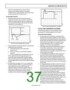
Power Circuitry
1. The switching power path on the PCB should be routed to
encompass the shortest possible length to minimize
radiated switching noise energy (that is, EMI) and
conduction losses in the board. Failure to take proper
precautions often results in EMI problems for the entire PC
system as well as noise-related operational problems in the
power-converter control circuitry. The switching power
path is the loop formed by the current path through the
input capacitors and the power MOSFETs, including all
interconnecting PCB traces and planes. The use of short,
wide interconnection traces is especially critical in this
path for two reasons: it minimizes the inductance in the
switching loop, which can cause high energy ringing, and it
accommodates the high current demand with minimal
voltage loss.
2. When a power-dissipating component (for example, a
power MOSFET) is soldered to a PCB, the liberal use of
vias, both directly on the mounting pad and immediately
surrounding it, is recommended. Two important reasons
for this are improved current rating through the vias and
improved thermal performance from vias extended to the
Signal Circuitry
1. The output voltage is sensed and regulated between the FB
and FBRTN pins, and the traces of these pins should be
connected to the signal ground of the load. To avoid
differential mode noise pickup in the sensed signal, the
loop area should be as small as possible. Therefore, the FB
and FBRTN traces should be routed adjacent to each other,
atop the power ground plane, and back to the controller.
2. The feedback traces from the switch nodes should be
connected as close as possible to the inductor. The CSREF
signal should be Kelvin connected to the center point of
the copper bar, which is the VCORE common node for the
inductors of all the phases.
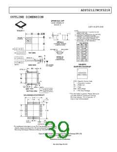
3. On the back of the ADP3212/NCP3218 package, there is a
metal pad that can be used to heat sink the device.
Therefore, running vias under the ADP3212/NCP3218 is
not recommended because the metal pad may cause
shorting between vias.
Rev. SpA | Page 38 of 43

 ONSEMI [ ONSEMI ]