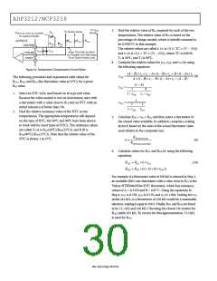
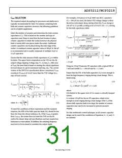
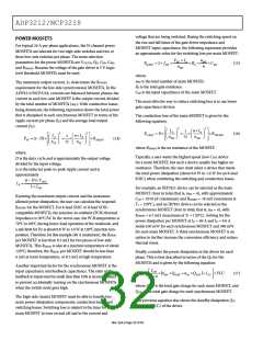
ADP3212/NCP3218
current slew rate, ensuring the optimal position and allowing
the minimization of the output decoupling.
1
(23)
(24)
fP0
=
2π(CA + CB )× RFB
With the multimode feedback structure of the
ADP3212/NCP3218, it is necessary to set the feedback
compensation so that the converter’s output impedance works
in parallel with the output decoupling. In addition, it is
necessary to compensate for the several poles and zeros created
by the output inductor and decoupling capacitors (output
filter).
CA + CB
2π× RA ×CB ×CA
fP1 =
The expressions that follow compute the time constants for
the poles and zeros in the system and are intended to yield an
optimal starting point for the design; some adjustments may be
necessary to account for PCB and component parasitic effects
(see the Tuning Procedure for 12 section):
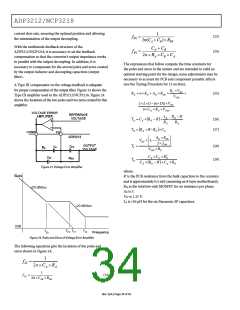
A Type III compensator on the voltage feedback is adequate
for proper compensation of the output filter. Figure 23 shows the
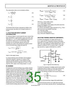
Type III amplifier used in the ADP3212/NCP3218. Figure 24
shows the locations of the two poles and two zeros created by this
amplifier.
RL ×VRT
VVID
RE = n×RO + AD ×RDS
+
+
(25)
2×L×(1−(n×D))×VRT
n×CX ×RO ×VVID
RO − R'
RX
LX
RO
TA = CX ×
(
RO − R'
)
+
×
(26)
(27)
TB =
RX + R'−RO
×CX
⎛
⎞
⎟
⎟
⎠
AD × RDS
2× fSW
⎜
V
RT × L −
⎜
⎝
TC =
(28)
(29)
V
VID × RE
CX ×C ×R2
Z
O
TD
where:
=
CX ×
(
RO − R' +CZ ×RO
)
Figure 23. Voltage Error Amplifier
R' is the PCB resistance from the bulk capacitors to the ceramics
and is approximately 0.4 mΩ (assuming an 8-layer motherboard).
R
DS is the total low-side MOSFET for on resistance per phase.
AD is 5.
RT is 1.25 V.
LX is 150 pH for the six Panasonic SP capacitors.
V
Figure 24. Poles and Zeros of Voltage Error Amplifier
The following equations give the locations of the poles and
zeros shown in Figure 24:
1
fZ1 =
(21)
(22)
2π×CA × RA
1
fZ2
=
2π×CFB ×RFB
Rev. SpA | Page 34 of 43

 ONSEMI [ ONSEMI ]