ADP3212/NCP3218
where:
LIM is the current limit resistor.
RO is the output load line.
LIM is the current limit setpoint.
RAMP RESISTOR SELECTION
R
The ramp resistor (RR) is used to set the size of the internal PWM
ramp. The value of this resistor is chosen to provide the best
combination of thermal balance, stability, and transient response.
Use the following expression to determine a starting value:
I
When the ADP3212/NCP3218 is configured for 3 phase
operation, the equation above is used to set the current limit.
When the ADP3212/NCP3218 switches from 3 phase to 1 phase
operation by PSI or DPRSLP signal, the current is single phase
is one third of the current limit in 3 phase.
AR × L
RR =
3× AD × RDS ×CR
(18)
0.5×360nH
3×5×5.2mΩ×5pF
RR =
= 462kΩ
When the ADP3212/NCP3218 is configured for 2 phase
operation, the equation above is used to set the current limit.
When the ADP3212/NCP3218 switches from 2 phase to 1 phase
operation by PSI or DPRSLP signal, the current is single phase
is one half of the current limit in 2 phase.
where:
AR is the internal ramp amplifier gain.
When the ADP3212/NCP3218 is configured for 1 phase
operation, the equation above is used to set the current limit.
AD is the current balancing amplifier gain.
R
DS is the total low-side MOSFET on resistance.
CR is the internal ramp capacitor value.
CURRENT MONITOR
Another consideration in the selection of RR is the size of the
internal ramp voltage (see Equation 19). For stability and noise
immunity, keep the ramp size larger than 0.5 V. Taking this into
consideration, the value of RR in this example is selected as 280 kΩ.
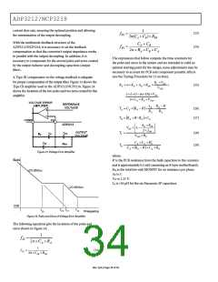
The ADP3212/NCP3218 has output current monitor. The
IMON pin sources a current proportional to the total inductor
current. A resistor, RMON, from IMON to FBRTN sets the gain
of the output current monitor. A 0.1 μF is placed in parallel with
RMON to filter the inductor current ripple and high frequency
load transients. Since the IMON pin is connected directly to the
CPU, it is clamped to prevent it from going above 1.15V.
The internal ramp voltage magnitude can be calculated as follows:
AR ×(1− D)×VVID
VR =
RR ×CR × fSW
The IMON pin current is equal to the RLIMtimes a fixed gain of
4. RMON can be found using the following equation:
(19)
0.5× (1− 0.061)×1.150 V
462kΩ×5pF× 280 kHz
VR =
= 0.83V
1.15V × RLIM
4× RO × IFS
(28)
RMON
=
where:
MON is the current monitor resistor. RMON is connected from
IMON pin to FBRTN.
RLIM is the current limit resistor.
RO is the output load line resistance.
IFS is the output current when the voltage on IMON is at full
scale.
The size of the internal ramp can be increased or decreased. If it
is increased, stability and transient response improves but
thermal balance degrades. Conversely, if the ramp size is
decreased, thermal balance improves but stability and transient
response degrade. In the denominator of Equation 18, the factor
of 3 sets the minimum ramp size that produces an optimal
combination of good stability, transient response, and thermal
balance.
R
FEEDBACK LOOP COMPENSATION DESIGN
CURRENT LIMIT SETPOINT
Optimized compensation of the ADP3212/NCP3218 allows the
best possible response of the regulator’s output to a load change.
The basis for determining the optimum compensation is to
make the regulator and output decoupling appear as an output
impedance that is entirely resistive over the widest possible
frequency range, including dc, and that is equal to the droop
resistance (RO). With the resistive output impedance, the output
voltage droops in proportion with the load current at any load
To select the current limit setpoint, the resistor value for RCLIM must
be determined. The current limit threshold for the
ADP3212/NCP3218 is set with RCLIM. RCLIM can be found using
the following equation:
ILIM × RO
(20)
RLIM
=
60μA
Rev. SpA | Page 33 of 43

 ONSEMI [ ONSEMI ]