ADP3212/NCP3218
conditions used for the single-point thermal monitoring
example—that is, an alarm temperature of 100°C and use of an
NTHS-0603N011003J Vishay thermistor—solving Equation 42
gives a RTTSET of 7.37 kΩ, and the closest standard resistor is
7.32 kΩ (1%).
6. Repeat Steps 4 and 5 until no adjustment of RPH is needed.
Once this is achieved, do not change RPH, RCS1, RCS2, or RTH
for the rest of the procedure.
7. Measure the output ripple with no load and with a full load
with scope, making sure both are within the specifications.
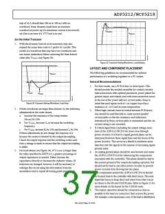
Set the AC Load Line
1. Remove the dc load from the circuit and connect a
dynamic load.
2. Connect the scope to the output voltage and set it to dc
coupling mode with a time scale of 100 μs/div.
3. Set the dynamic load for a transient step of about 40 A at
1 kHz with 50% duty cycle.
4. Measure the output waveform (note that use of a dc offset
on the scope may be necessary to see the waveform). Try to
use a vertical scale of 100 mV/div or finer.
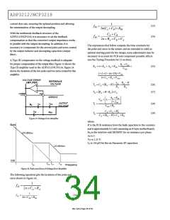
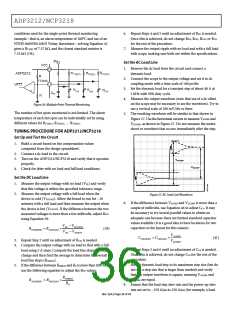
Figure 26. Multiple-Point Thermal Monitoring
The number of hot spots monitored is not limited. The alarm
temperature of each hot spot can be individually set by using
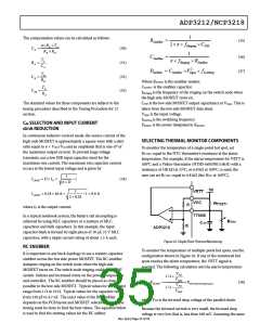
5. The resulting waveform will be similar to that shown in
Figure 27. Use the horizontal cursors to measure VACDRP and
different values for RTTSET1, RTTSET2, … RTTSETn
.
VDCDRP, as shown in Figure 27. Do not measure the under-
shoot or overshoot that occurs immediately after the step.
TUNING PROCEDURE FOR ADP3212/NCP321±
Set Up and Test the Circuit
1. Build a circuit based on the compensation values
computed from the design spreadsheet.
2. Connect a dc load to the circuit.
3. Turn on the ADP3212/NCP3218 and verify that it operates
V
ACDRP
properly.
V
DCDRP
4. Check for jitter with no load and full load conditions.
Set the DC Load Line
1. Measure the output voltage with no load (VNL) and verify
that this voltage is within the specified tolerance range.
2. Measure the output voltage with a full load when the
device is cold (VFLCOLD). Allow the board to run for ~10
minutes with a full load and then measure the output when
the device is hot (VFLHOT). If the difference between the two
measured voltages is more than a few millivolts, adjust RCS2
using Equation 39.
Figure 27. AC Load Line Waveform
6. If the difference between VACDRP and VDCDRP is more than a
couple of millivolts, use Equation 46 to adjust CCS. It may
be necessary to try several parallel values to obtain an
adequate one because there are limited standard capacitor
values available (it is a good idea to have locations for two
capacitors in the layout for this reason).
VNL −VFLCOLD
VNL −VFLHOT
RCS2(NEW) = RCS2(OLD)
×
(39)
VACDRP
VDCDRP
CCS(NEW) = CCS(OLD)
×
(41)
3. Repeat Step 2 until no adjustment of RCS2 is needed.
4. Compare the output voltage with no load to that with a full
load using 5 A steps. Compute the load line slope for each
change and then find the average to determine the overall
load line slope (ROMEAS).
5. If the difference between ROMEAS and RO is more than 0.05 mΩ,
use the following equation to adjust the RPH values:
7. Repeat Steps 5 and 6 until no adjustment of CCS is needed.
Once this is achieved, do not change CCS for the rest of the
procedure.
8. Set the dynamic load step to its maximum step size (but do
not use a step size that is larger than needed) and verify
that the output waveform is square, meaning VACDRP and
ROMEAS
RO
VDCDRP are equal.
RPH(NEW) = RPH(OLD)
×
(40)
9. Ensure that the load step slew rate and the power-up slew
rate are set to ~150 A/μs to 250 A/μs (for example, a load
Rev. SpA | Page 36 of 43

 ONSEMI [ ONSEMI ]