ADP3212/NCP3218
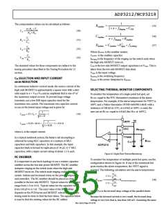
step of 50 A should take 200 ns to 300 ns) with no
overshoot. Some dynamic loads have an excessive
overshoot at power-up if a minimum current is incorrectly
set (this is an issue if a VTT tool is in use).
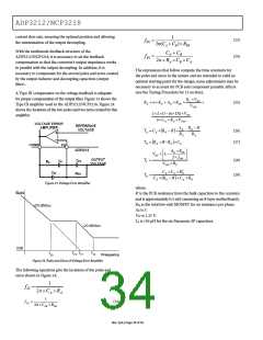
V
TRANREL
V
DROOP
Set the Initial Transient
1. With the dynamic load set at its maximum step size,
expand the scope time scale to 2 μs/div to 5 μs/div. This
results in a waveform that may have two overshoots and
one minor undershoot before achieving the final desired
value after VDROOP (see Figure 28).
Figure 29. Transient Setting Waveform, Load Release
LAYOUT AND COMPONENT PLACEMENT
The following guidelines are recommended for optimal
performance of a switching regulator in a PC system.
V
DROOP
General Recommendations
1. For best results, use a PCB of four or more layers. This
should provide the needed versatility for control circuitry
interconnections with optimal placement; power planes for
ground, input, and output; and wide interconnection traces
in the rest of the power delivery current paths. Keep in
mind that each square unit of 1 oz copper trace has a
resistance of ~0.53 mΩ at room temperature.
2. When high currents must be routed between PCB layers,
vias should be used liberally to create several parallel
current paths so that the resistance and inductance
introduced by these current paths is minimized and the via
current rating is not exceeded.
3. If critical signal lines (including the output voltage sense
lines of the ADP3212/NCP3218) must cross through
power circuitry, it is best if a signal ground plane can be
interposed between those signal lines and the traces of the
power circuitry. This serves as a shield to minimize noise
injection into the signals at the expense of increasing signal
ground noise.
4. An analog ground plane should be used around and under
the ADP3212/NCP3218 for referencing the components
associated with the controller. This plane should be tied to
the nearest ground of the output decoupling capacitor, but
should not be tied to any other power circuitry to prevent
power currents from flowing into the plane.
V
TRAN1
V
TRAN2
Figure 28. Transient Setting Waveform, Load Step
2. If both overshoots are larger than desired, try the following
adjustments in the order shown.
a. Increase the resistance of the ramp resistor
(RRAMP) by 25%.
b. For VTRAN1, increase CB or increase the switching
frequency.
c. For VTRAN2, increase RA by 25% and decrease CA by 25%.
If these adjustments do not change the response, it is
because the system is limited by the output decoupling.
Check the output response and the switching nodes each
time a change is made to ensure that the output decoupling
is stable.
3. For load release (see Figure 29), if VTRANREL is larger than
the value specified by IMVP-6.5, a greater percentage of
output capacitance is needed. Either increase the
capacitance directly or decrease the inductor values. (If
inductors are changed, however, it will be necessary to
redesign the circuit using the information from the
spreadsheet and to repeat all tuning guide procedures).
5. The components around the ADP3212/NCP3218 should
be located close to the controller with short traces. The most
important traces to keep short and away from other traces
are those to the FB and CSSUM pins. Refer to Figure 22 for
more details on the layout for the CSSUM node.
6. The output capacitors should be connected as close as
possible to the load (or connector) that receives the power
(for example, a microprocessor core). If the load is distributed,
Rev. SpA | Page 37 of 43

 ONSEMI [ ONSEMI ]