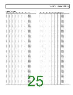
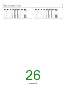
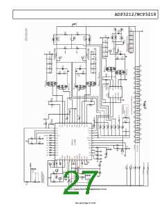
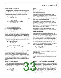
ADP3212/NCP3218
The output current is measured by summing the currents of the
resistors monitoring the voltage across each inductor and by
passing the signal through a low-pass filter. The summing is
implemented by the CS amplifier that is configured with resistor
VVID × RO ×(1− (n× DMIN ))
fSW ×VRIPPLE
(5)
L ≥
Solving Equation 5 for a 16 mV peak-to-peak output ripple
voltage yields
RPH(x) (summer) and resistors RCS and CCS (filters). The output
resistance of the regulator is set by the following equations:
1.05 V ×1.9 mΩ ×
(
1− 2×0.055
)
L ≥
= 528 nH
RCS
RPH(x)
300 kHz×16 mV
RO
=
×RSENSE
(6)
(7)
If the resultant ripple voltage is less than the initially selected
L
value, the inductor can be changed to a smaller value until the
ripple value is met. This iteration allows optimal transient
response and minimum output decoupling.
CCS
=
R
SENSE × RCS
where RSENSE is the DCR of the output inductors.
The smallest possible inductor should be used to minimize the
number of output capacitors. Choosing a 490 nH inductor is a
good choice for a starting point, and it provides a calculated
ripple current of 9.0 A. The inductor should not saturate at the
peak current of 24.5 A, and it should be able to handle the sum
of the power dissipation caused by the winding’s average current
(20 A) plus the ac core loss. In this example, 330 nH is used.
Either RCS or RPH(x) can be chosen for added flexibility. Due to
the current drive ability of the CSCOMP pin, the RCS resistance
should be greater than 100 kΩ. For example, initially select RCS
to be equal to 200 kΩ, and then use Equation 7 to solve for CCS:
330 nH
0.8 mꢁ × 200 kꢁ
CCS
=
= 2.1nF
Another important factor in the inductor design is the DCR,
which is used for measuring the phase currents. Too large of a
DCR causes excessive power losses, whereas too small of a value
leads to increased measurement error. For this example, an
inductor with a DCR of 0.8 mΩ is used.
If CCS is not a standard capacitance, RCS can be tuned. For
example, if the optimal CCS capacitance is 1.5 nF, adjust RCS to
280 kΩ. For best accuracy, CCS should be a 5% NPO capacitor.
In this example, a 220 kΩ is used for RCS to achieve optimal results.
Selecting a Standard Inductor
Next, solve for RPH(x) by rearranging Equation 6 as follows:
0.8 mꢁ
After the inductance and DCR are known, select a standard
inductor that best meets the overall design goals. It is also
important to specify the inductance and DCR tolerance to
maintain the accuracy of the system. Using 20% tolerance for
the inductance and 15% for the DCR at room temperature are
reasonable values that most manufacturers can meet.
RPH(x)
≥
×220 kꢁ = 83.8 kꢁ
2.1 mꢁ
The standard 1% resistor for RPH(x) is 86.6 kΩ.
Inductor DCR Temperature Correction
If the DCR of the inductor is used as a sense element and
copper wire is the source of the DCR, the temperature changes
associated with the inductor’s winding must be compensated
for. Fortunately, copper has a well-known temperature
coefficient (TC) of 0.39%/°C.
Power Inductor Manufacturers
The following companies provide surface-mount power inductors
optimized for high power applications upon request:
•
•
•
•
Vishay Dale Electronics, Inc.
(605) 665-9301
Panasonic
(714) 373-7334
Sumida Electric Company
(847) 545-6700
If RCS is designed to have an opposite but equal percentage of
change in resistance, it cancels the temperature variation of the
inductor’s DCR. Due to the nonlinear nature of NTC thermistors,
series resistors RCS1 and RCS2 (see Figure 22) are needed to linearize
the NTC and produce the desired temperature coefficient tracking.
NEC Tokin Corporation
(510) 324-4110
Output Droop Resistance
The design requires that the regulator output voltage measured
at the CPU pins decreases when the output current increases. The
specified voltage drop corresponds to the droop resistance (RO).
Rev. SpA | Page 29 of 43

 ONSEMI [ ONSEMI ]