Functional Description (Continued)
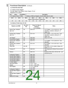
13.0 REGISTERS AND RAM
13.1 Address Pointer Register
The main register is the Address Pointer Register. The bit
designations are as follows:
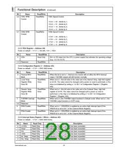
Bit
Name
Read/Write
Description
7-0 Address Pointer
Write
Address of RAM and Registers. See the tables below for detail.
Bit 7
Bit 6
A6
Bit 5
Bit 4
Address Pointer (Power On default 00h)
A4 A3
Bit 3
Bit 2
Bit 1
Bit 0
A7
A5
A2
A1
A0
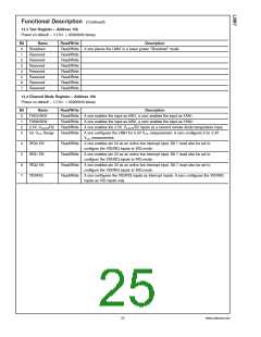
13.2 Address Pointer Index (A7–A0)
A6–A0 in
Hex
Power On Value of
Registers:
Registers and RAM
Notes
<
>
7:0 in Binary
<
>
Internal Temp. Hardware
High Limit
13h
14h
0100 0110
70 ˚C Default - 7:0 =0100 0110 - User
adjustable. Lockable by setting bit 1 of
register 4Ah.
<
>
External Temp. Hardware
High Limit
0101 0101
85 ˚C Default - 7:0 =0101 0101 - User
adjustable. Lockable by setting bit 2 of
register 4Ah.
Test Register
15h
16h
17h
0000 0000
0000 0000
0100 0110
Always set to 00h
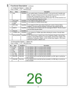
Channel Mode Register
Internal Temp. Hardware
High Limit
<
>
70 ˚C Default - 7:0 =0100 0110 - User
adjustable
<
>
External Temp. Hardware
High Limit
18h
0101 0101
85 ˚C Default - 7:0 =0101 0101 - User
adjustable
Value RAM
19h–3Dh
3Eh
See Section 13.18 for details. Address 19h
default=1111 1111
Company ID
Revision
0000 0010
0000 0110
This designates the National Semiconductor
LM87.
3Fh
Revisions of this device will start with 1 and
increment by one.
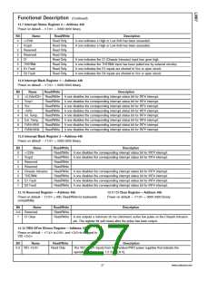
Configuration Register 1
Interrupt Status Register 1
Interrupt Status Register 2
Interrupt Mask Register 1
Interrupt Mask Register 2
CI Clear Register
40h
41h
42h
43h
44h
46h
47h
0000 1000
0000 0000
0000 0000
0000 0000
0000 0000
0000 0000
<
<
<
>
7:4 = 0101;
VID0-3/Fan Divisor
Register
>
3:0 = VID3–VID0
>
7:1 =1000 000;
VID4 Register
49h
< >
0
=VID4
Configuration Register 2
Interrupt Status Register 1
Mirror
4Ah
4Ch
0000 0000
0000 0000
Interrupt Status Register 2
Mirror
4Dh
80h
0000 0000
0010 0000
SMBALERT# Enable
www.national.com
24

 NSC [ National Semiconductor ]