Functional Description (Continued)
13.7 Interrupt Status Register 2—Address 42h
<
>
Power on default – 7:0 = 0000 0000 binary
Bit
0
Name
+12Vin
Read/Write
Read Only
Read Only
Read Only
Read Only
Read Only
Read Only
Read Only
Read Only
Description
A one indicates a High or Low limit has been exceeded.
A one indicates a High or Low limit has been exceeded.
1
Vccp2
2
Reserved
Reserved
CI
3
4
A one indicates the CI (Chassis Intrusion) input has gone high.
A one indicates the THERM# input has been pulled low by external circuitry.
A one indicates the D1 inputs are shorted to Vcc or open circuit.
A one indicates the D2 inputs are shorted to Vcc or open circuit.
5
THERM#
D1 Fault
D2 Fault
6
7
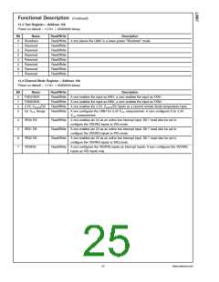
13.8 Interrupt Mask Register 1—Address 43h
<
>
Power on default – 7:0 = 0000 0000 binary
Bit
0
Name
Read/Write
Description
#
+2.5Vin/D2+ Read/Write A one disables the corresponding interrupt status bit for INT interrupt.
#
Read/Write A one disables the corresponding interrupt status bit for INT interrupt.
1
Vccp1
#
Read/Write A one disables the corresponding interrupt status bit for INT interrupt.
2
Vcc
#
Read/Write A one disables the corresponding interrupt status bit for INT interrupt.
3
+5Vin
#
Read/Write A one disables the corresponding interrupt status bit for INT interrupt.
4
Int. Temp.
Ext. Temp.
FAN1/AIN1
FAN2/AIN2
#
Read/Write A one disables the corresponding interrupt status bit for INT interrupt.
5
#
Read/Write A one disables the corresponding interrupt status bit for INT interrupt.
6
#
Read/Write A one disables the corresponding interrupt status bit for INT interrupt.
7
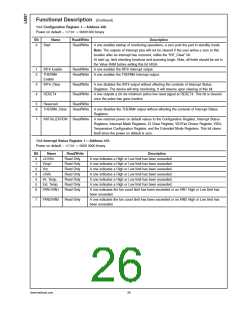
13.9 Interrupt Mask Register 2—Address 44h
<
>
Power on default – 7:0 = 0000 0000 binary
Bit
0
Name
+12Vin
Read/Write
Description
#
Read/Write A one disables the corresponding interrupt status bit for INT interrupt.
#
1
Vccp2
Read/Write A one disables the corresponding interrupt status bit for INT interrupt.
2
Reserved
Reserved
Chassis Intrusion
THERM#
D1 Fault
Read/Write
Read/Write
3
#
Read/Write A one disables the corresponding interrupt status bit for INT interrupt.
4
#
Read/Write A one disables the corresponding interrupt status bit for INT interrupt.
5
#
Read/Write A one disables the corresponding interrupt status bit for INT interrupt.
6
#
7
D2 Fault
Read/Write A one disables the corresponding interrupt status bit for INT interrupt.
13.10 Reserved Register —Address 45h
13.11 CI Clear Register—Address 46h
<
>
<
>
Power on default – 7:0 = 00h. Read/Write for backwards
compatibility.
Power on default – 7:0 = 0000 0000 binary
Bit
0-6 Reserved
CI Clear
Name
Read/Write
Description
Read/Write
7
Read/Write A one outputs a minimum 20 ms (minimum) active low pulse on the Chassis Intrusion
pin. The register bit self clears after the pulse has been output.
13.12 VID0-3/Fan Divisor Register—Address 47h
<
>
<
>
Power on default – 7:4 is 0101, and 3:0 is mapped to
<
>
VID 3:0
Bit
Name
Read/Write
Description
<
>
<
>
0-3 VID 3:0
Read Only
The VID 3:0 inputs from the Pentium/PRO power supplies that indicate the
operating voltage (e.g. 1.5 V to 2.9 V).
27
www.national.com

 NSC [ National Semiconductor ]