30086725
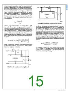
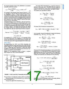
FIGURE 10. MOSFET Power Up Waveforms
MOSFET SELECTION
must be at least 260 mA to conduct the GATE pull-down cur-
rent when a circuit breaker condition is detected.
It is recommended that the external MOSFET (Q1) selection
be based on the following criteria:
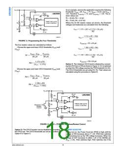
TIMER CAPACITOR, CT
-
The BVDSS rating should be greater than the maximum
The TIMER pin capacitor (CT) sets the timing for the insertion
time delay, fault timeout period, and restart timing of the
LM25069-2.
system voltage (VSYS), plus ringing and transients which can
occur at VSYS when the circuit card, or adjacent cards, are
inserted or removed.
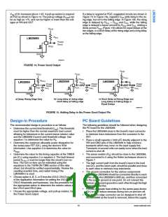
A) Insertion Delay - Upon applying the system voltage
(VSYS) to the circuit, the external MOSFET (Q1) is held off
during the insertion time (t1 in Figure 3) to allow ringing and
transients at VSYS to settle. Since each backplane’s response
to a circuit card plug-in is unique, the worst case settling time
must be determined for each application. The insertion time
starts when VIN reaches the POR threshold, at which time the
internal 5.5 µA current source charges CT from 0V to 1.72V.
The required capacitor value is calculated from:
-
The maximum continuous current rating should be based
on the current limit threshold (50 mV/RS), not the maximum
load current, since the circuit can operate near the current
limit threshold continuously.
-
The Pulsed Drain Current spec (IDM) must be greater than
the current threshold for the circuit breaker function (95 mV/
RS).
-
The SOA (Safe Operating Area) chart of the device, and
the thermal properties, should be used to determine the max-
imum power dissipation threshold set by the RPWR resistor.
The programmed maximum power dissipation should have a
reasonable margin from the maximum power defined by the
FET's SOA chart if the LM25069-2 is used since the FET will
be repeatedly stressed during fault restart cycles. The FET
manufacturer should be consulted for guidelines.
For example, if the desired insertion delay is 250 ms, CT cal-
culates to 0.8 µF. At the end of the insertion delay, CT is
quickly discharged by a 2 mA current sink.
-
RDS(on) should be sufficiently low that the power dissipa-
tion at maximum load current (IL(max)2 x RDS(on)) does not raise
its junction temperature above the manufacturer’s recom-
mendation.
B) Fault Timeout Period - During in-rush current limiting or
upon detection of a fault condition where the current limit and/
or power limit circuits regulate the current through Q1, the
fault timer current source (80 µA) switches on to charge CT.
The Fault Timeout Period is the time required for the voltage
at the TIMER pin to transition from ground to 1.72V, at which
time Q1 is switched off. If the LM25069-1 is in use, the re-
quired capacitor value is calculated from:
If the circuit’s input voltage is at the low end of the LM25069’s
operating range (<3.5V), or at the high end of the operating
range (>14V), the gate-to-source voltage applied to the MOS-
FET by the LM25069 is less than 5V, and can approach 1V
in a worst case situation. See the graph “GATE Pin Voltage”.
The selected device must have a suitable Gate-to-Source
Threshold Voltage.
The gate-to-source voltage provided by the LM25069 can be
as high as 19.5V at turn-on when the output voltage is zero.
At turn-off the reverse gate-to-source voltage will be equal to
the output voltage at the instant the GATE pin is pulled low.
If the device chosen for Q1 is not rated for these voltages, an
external zener diode must be added from its gate to source,
with the zener voltage less than the device maximum VGS
rating. The zener diode’s working voltage protects the MOS-
FET during turn-on, and its forward voltage protects the MOS-
FET during shutoff. The zener diode’s forward current rating
(3)
For example, if the desired Fault Timeout Period is 17 ms,
CT calculates to 0.8 µF. When the Fault Timeout Period ex-
pires, the LM25069-1 latches the GATE pin low until a power-
up sequence is initiated by external circuitry. If the LM25069-2
is in use, the Fault Timeout Period during restart cycles is
approximately 18% shorter than the initial fault timeout period
which initiated the restart cycles since the voltage at the
TIMER pin transitions from 0.3V to 1.72V. Since the Fault
Timeout Period must always be longer than the turn-on-time,
www.national.com
16

 NSC [ National Semiconductor ]