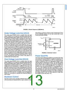
30086716
FIGURE 5. Restart Sequence (LM25069-2)
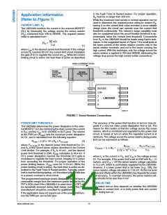
drain device, as shown in Figure 6. Upon releasing the UVLO
pin the LM25069 switches on the load current with in-rush
current and power limiting.
Under-Voltage Lock-Out (UVLO)
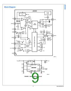
The series pass MOSFET (Q1) is enabled when the input
supply voltage (VSYS) is within the operating range defined by
the programmable under-voltage lockout (UVLO) and over-
voltage lock-out (OVLO) levels. Typically the UVLO level at
VSYS is set with a resistor divider (R1-R3) as shown in Figure
1. Refering to the Block Diagram when VSYS is below the UV-
LO level, the internal 20 µA current source at UVLO is en-
abled, the current source at OVLO is off, and Q1 is held off
by the 2 mA pull-down current at the GATE pin. As VSYS is
increased, raising the voltage at UVLO above its threshold the
20 µA current source at UVLO is switched off, increasing the
voltage at UVLO, providing hysteresis for this threshold. With
the UVLO pin above its threshold, Q1 is switched on by the
20 µA current source at the GATE pin if the insertion time
delay has expired. See the Applications Section for a proce-
dure to calculate the values of the threshold setting resistors
(R1-R3). The minimum possible UVLO level at VSYS can be
set by connecting the UVLO pin to VIN. In this case Q1 is
enabled after the insertion time.
30086717
FIGURE 6. Shutdown Control
Power Good Pin
The Power Good indicator pin (PGD) is connected to the drain
of an internal N-channel MOSFET capable of sustaining 17V
in the off-state, and transients up to 20V. An external pull-up
resistor is required at PGD to an appropriate voltage to indi-
cate the status to downstream circuitry. The off-state voltage
at the PGD pin can be higher or lower than the voltages at
VIN and OUT. PGD is switched high when the voltage from
SENSE to OUT (the external MOSFET’s VDS) decreases be-
low 1.3V. PGD switches low when the MOSFET’s VDS is
increased past 1.9V. If the UVLO pin is taken below its thresh-
old or the OVLO pin taken above its threshold, to disable the
LM25069, PGD switches low within 10 µs without waiting for
the voltage at OUT to fall. The PGD output pin is high when
the voltage at VIN is less than 1.6V.
Over-Voltage Lock-Out (OVLO)
The series pass MOSFET (Q1) is enabled when the input
supply voltage (VSYS) is within the operating range defined by
the programmable under-voltage lockout (UVLO) and over-
voltage lock-out (OVLO) levels. If VSYS raises the OVLO pin
voltage above its threshold Q1 is switched off by the 2 mA
pull-down current at the GATE pin, denying power to the load.
When the OVLO pin is above its threshold, the internal 20 µA
current source at OVLO is switched on, raising the voltage at
OVLO to provide threshold hysteresis. When VSYS is reduced
below the OVLO level Q1 is enabled. See the Applications
Section for a procedure to calculate the threshold setting re-
sistor values.
Shutdown Control
The load current can be remotely switched off by taking the
UVLO pin below its threshold with an open collector or open
13
www.national.com

 NSC [ National Semiconductor ]