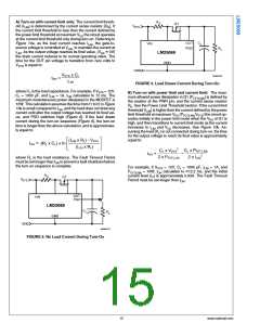
VDS of Q1 increases above 1.9V. A pull-up resistor is required
at PGD as shown in Figure 14. The pull-up voltage (VPGD) can
be as high as 17V, and can be higher or lower than the volt-
ages at VIN and OUT.
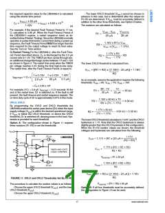
If a delay is required at PGD, suggested circuits are shown in
Figure 15. In Figure 15a, capacitor CPG adds delay to the ris-
ing edge, but not to the falling edge. In Figure 15b, the rising
edge is delayed by RPG1 + RPG2 and CPG, while the falling
edge is delayed a lesser amount by RPG2 and CPG. Adding a
diode across RPG2 (Figure 15c) allows for equal delays at the
two edges, or a short delay at the rising edge and a long delay
at the falling edge.
30086751
FIGURE 14. Power Good Output
30086752
FIGURE 15. Adding Delay to the Power Good Output Pin
Design-in Procedure
PC Board Guidelines
The recommended design-in procedure is as follows:
The following guidelines should be followed when designing
the PC board for the LM25069:
•
Determine the current limit threshold (ILIM). This threshold
must be higher than the normal maximum load current,
allowing for tolerances in the current sense resistor value
and the LM25069 Current Limit threshold voltage. Use
equation 1 to determine the value for RS.
•
Place the LM25069 close to the board’s input connector
to minimize trace inductance from the connector to the
FET.
•
Place a small capacitor (1000 pF) directly adjacent to the
VIN and GND pins of the LM25069 to help minimize
transients which may occur on the input supply line.
Transients of several volts can easily occur when the load
current is shut off.
•
•
Determine the maximum allowable power dissipation for
the series pass FET (Q1), using the device’s SOA
information. Use equation 2 to determine the value for
RPWR
.
Determine the value for the timing capacitor at the TIMER
pin (CT) using equation 3 or equation 4. The fault timeout
period (tFAULT) must be longer than the circuit’s turn-on-
time. The turn-on time can be estimated using the
equations in the TURN-ON TIME section of this data
sheet, but should be verified experimentally. Review the
resulting insertion time, and restart timing if the
LM25069-2 is used.
•
•
•
The sense resistor (RS) should be close to the LM25069,
and connected to it using the Kelvin techniques shown in
Figure 7.
The high current path from the board’s input to the load
(via Q1), and the return path, should be parallel and close
to each other to minimize loop inductance.
The ground connection for the various components
around the LM25069 should be connected directly to each
other, and to the LM25069’s GND pin, and then connected
to the system ground at one point. Do not connect the
various component grounds to each other through the high
current ground line.
•
•
Choose option A, B, C, or D from the UVLO, OVLO section
of the Application Information for setting the UVLO and
OVLO thresholds and hysteresis. Use the procedure for
the appropriate option to determine the resistor values at
the UVLO and OVLO pins.
•
•
Provide adequate heat sinking for the series pass device
(Q1) to help reduce stresses during turn-on and turn-off.
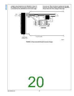
The board’s edge connector can be designed to shut off
the LM25069 as the board is removed, before the supply
Choose the appropriate voltage, and pull-up resistor, for
the Power Good output.
19
www.national.com

 NSC [ National Semiconductor ]