30086713
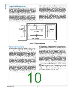
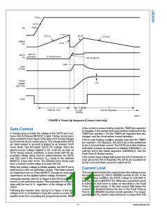
FIGURE 3. Power Up Sequence (Current Limit only)
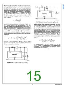
in the current or power limiting mode the TIMER pin capacitor
is charging. If the current and power limiting cease before the
TIMER pin reaches 1.72V the TIMER pin capacitor then dis-
charges, and the circuit enters normal operation.
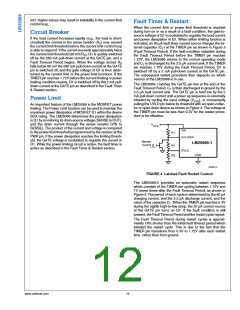
Gate Control
A charge pump provides the voltage at the GATE pin to en-
hance the N-Channel MOSFET’s gate. During normal oper-
ating conditions (t3 in Figure 3) the gate of Q1 is held charged
by an internal 20 µA current source. The voltage at the GATE
pin (with respect to ground) is limited by an internal 19.5V
zener diode. See the graph “GATE Pin voltage. Since the
gate-to-source voltage applied to Q1 could be as high as
19.5V during various conditions, a zener diode with the ap-
propriate voltage rating must be added between the GATE
and OUT pins if the maximum VGS rating of the selected
MOSFET is less than 19.5V. The external zener diode must
have a forward current rating of at least 260 mA.
If the in-rush limiting condition persists such that the TIMER
pin reached 1.72V during t2, the GATE pin is then pulled low
by the 2 mA pull-down current. The GATE pin is then held low
until either a power up sequence is initiated (LM25069-1), or
until the end of the restart sequence (LM25069-2). See the
Fault Timer & Restart section.
If the system input voltage falls below the UVLO threshold, or
rises above the OVLO threshold, the GATE pin is pulled low
by the 2 mA pull-down current to switch off Q1.
When the system voltage is initially applied, the GATE pin is
held low by a 260 mA pull-down current. This helps prevent
an inadvertent turn-on of the MOSFET through its drain-gate
capacitance as the applied system voltage increases.
Current Limit
The current limit threshold is reached when the voltage across
the sense resistor RS (VIN to SENSE) reaches 50 mV. In the
current limiting condition, the GATE voltage is controlled to
limit the current in MOSFET Q1. While the current limit circuit
is active, the fault timer is active as described in the Fault
Timer & Restart section. If the load current falls below the
current limit threshold before the end of the Fault Timeout
Period, the LM25069 resumes normal operation. For proper
operation, the RS resistor value should be no larger than 200
During the insertion time (t1 in Figure 3) the GATE pin is held
low by a 2 mA pull-down current. This maintains Q1 in the off-
state until the end of t1, regardless of the voltage at VIN or
UVLO.
Following the insertion time, during t2 in Figure 3, the gate
voltage of Q1 is modulated to keep the current or power dis-
sipation level from exceeding the programmed levels. While
11
www.national.com

 NSC [ National Semiconductor ]