of time results in the shutdown of the series pass device. In
this event, the LM25069-1 latches off until the circuit is re-
enabled by external control, while the LM25069-2 automati-
cally restarts with defined timing. The circuit breaker function
quickly switches off the series pass device upon detection of
a severe over-current condition. The Power Good (PGD) out-
put pin indicates when the output voltage is within 1.3V of the
system input voltage (VSYS). Programmable under-voltage
lock-out (UVLO) and over-voltage lock-out (OVLO) circuits
enable the LM25069 when the system input voltage is be-
tween the desired thresholds. The typical configuration of a
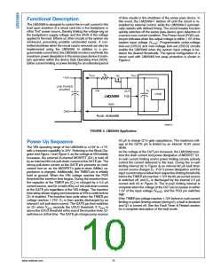
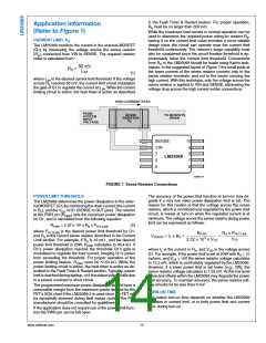
circuit card with LM25069 hot swap protection is shown in
Figure 2.
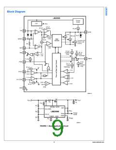
Functional Description
The LM25069 is designed to control the in-rush current to the
load upon insertion of a circuit card into a live backplane or
other "hot" power source, thereby limiting the voltage sag on
the backplane’s supply voltage, and the dV/dt of the voltage
applied to the load. Effects on other circuits in the system are
minimized, preventing possible unintended resets. A con-
trolled shutdown when the circuit card is removed can also be
implemented using the LM25069. In addition to a pro-
grammable current limit, the LM25069 monitors and limits the
maximum power dissipation in the series pass device to main-
tain operation within the device Safe Operating Area (SOA).
Either current limiting or power limiting for an extended period
30086712
FIGURE 2. LM25069 Application
20 µA to charge Q1’s gate capacitance. The maximum volt-
age at the GATE pin is limited by an internal 19.5V zener
diode.
Power Up Sequence
The VIN operating range of the LM25069 is +2.9V to +17V,
with a transient capability to 20V. Referring to the Block Dia-
gram and Figure 1 and Figure 3, as the voltage at VIN initially
increases, the external N-channel MOSFET (Q1) is held off
by an internal 260 mA pull-down current at the GATE pin. The
strong pull-down current at the GATE pin prevents an inad-
vertent turn-on as the MOSFET’s gate-to-drain (Miller) ca-
pacitance is charged. Additionally, the TIMER pin is initially
held at ground. When the VIN voltage reaches the POR
threshold the insertion time begins. During the insertion time,
the capacitor at the TIMER pin (CT) is charged by a 5.5 µA
current source, and Q1 is held off by a 2 mA pull-down current
at the GATE pin regardless of the VIN voltage. The insertion
time delay allows ringing and transients at VIN to settle before
Q1 is enabled. The insertion time ends when the TIMER pin
voltage reaches 1.72V. CT is then quickly discharged by an
internal 2 mA pull-down current. The GATE pin then switches
on Q1 when VSYS exceeds the UVLO threshold. If VSYS is
above the UVLO threshold at the end of the insertion time, Q1
switches on at that time. The GATE pin charge pump sources
As the voltage at the OUT pin increases, the LM25069 mon-
itors the drain current and power dissipation of MOSFET Q1.
In-rush current limiting and/or power limiting circuits actively
control the current delivered to the load. During the in-rush
limiting interval (t2 in Figure 3) an internal 80 µA fault timer
current source charges CT. If Q1’s power dissipation and the
input current reduce below their respective limiting thresholds
before the TIMER pin reaches 1.72V the 80 µA current source
is switched off, and CT is discharged by the internal 2.5 µA
current sink (t3 in Figure 3). The in-rush limiting interval is
complete when the voltage at the OUT pin increases to within
1.3V of the input voltage (VSYS), and the PGD pin switches
high.
If the TIMER pin voltage reaches 1.72V before in-rush current
limiting or power limiting ceases (during t2), a fault is declared
and Q1 is turned off. See the Fault Timer & Restart section
for a complete description of the fault mode.
www.national.com
10

 NSC [ National Semiconductor ]