Nexperia
PXN012-60QL
N-channel 60 V, 11.5 mOhm, logic level Trench MOSFET in MLPAK33
Symbol
Parameter
Conditions
Min
Typ
Max
Unit
Qoss
output charge
VGS = 0 V; VDS = 30 V; f = 1 MHz;
Tj = 25 °C
-
18
-
nC
Source-drain diode
VSD
trr
source-drain voltage
IS = 10 A; VGS = 0 V; Tj = 25 °C; Fig. 14
-
-
-
0.82
22.1
13
1.2
V
reverse recovery time IS = 10 A; dIS/dt = -100 A/µs; VGS = 0 V;
-
-
ns
nC
VDS = 30 V; Tj = 25 °C; Fig. 15
Qr
recovered charge
[1]
[1] includes capacitive recovery
aaa-033428
aaa-032715
80
75
10 V
V
= 4.5 V
I
D
R
GS
DSon
(A)
(mΩ)
60
45
30
15
0
60
40
20
0
3.5 V
3 V
2.8 V
2.6 V
0
0.5
1
1.5
2
2.5
3
DS
3.5
(V)
4
0
2
4
6
8
10
12
V
GS
14
(V)
16
V
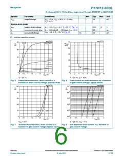
Tj = 25 °C
Tj = 25 °C; ID = 10 A
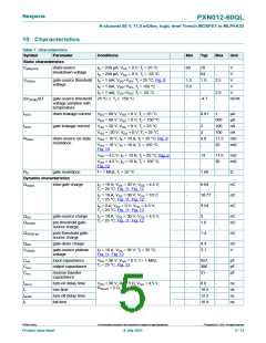
Fig. 5. Output characteristics; drain current as a
function of drain-source voltage; typical values
Fig. 6. Drain-source on-state resistance as a function
of gate-source voltage; typical values
aaa-032716
aaa-033429
-1
100
10
I
D
I
D
(A)
(A)
-2
-3
-4
-5
-6
80
60
40
20
0
10
10
10
10
10
150°C
T = 25°C
j
0
0.5
1
1.5
2
2.5
3
3.5
(V)
4
0
0.5
1
1.5
2
2.5
(V)
3
V
GS
V
GS
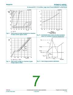
VDS = 8 V
Tj = 25 °C; VDS = 5 V
Fig. 7. Transfer characteristics; drain current as a
function of gate-source voltage; typical values
Fig. 8. Sub-threshold drain current as a function of
gate-source voltage
©
PXN012-60QL
All information provided in this document is subject to legal disclaimers.
Nexperia B.V. 2021. All rights reserved
Product data sheet
8 July 2021
6 / 12

 NEXPERIA [ Nexperia ]