Nexperia
PXN012-60QL
N-channel 60 V, 11.5 mOhm, logic level Trench MOSFET in MLPAK33
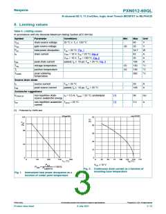
8. Limiting values
Table 5. Limiting values
In accordance with the Absolute Maximum Rating System (IEC 60134).
Symbol
VDS
VGS
Ptot
Parameter
Conditions
Min
Max
60
Unit
V
drain-source voltage
gate-source voltage
total power dissipation
drain current
25 °C ≤ Tj ≤ 150 °C
-
-20
20
V
Tsp = 25 °C; Fig. 1
-
34.7
42
W
A
ID
VGS = 10 V; Tsp = 25 °C; Fig. 2
VGS = 10 V; Tsp = 100 °C; Fig. 2
pulsed; tp ≤ 10 µs; Tsp = 25 °C; Fig. 3
-
-
26
A
IDM
peak drain current
storage temperature
junction temperature
-
168
150
150
260
A
Tstg
Tj
-55
-55
-
°C
°C
°C
Tsld(M)
peak soldering
temperature
Source-drain diode
IS
source current
peak source current
Tsp = 25 °C
-
-
29
A
A
ISM
pulsed; tp ≤ 10 µs; Tsp = 25 °C
168
Avalanche ruggedness
EDS(AL)S non-repetitive drain-
source avalanche energy
ID = 3.5 A; Tj(init) = 25 °C; unclamped
[1]
[1]
-
-
90
mJ
A
IAS
non-repetitive avalanche Tj(init) = 25 °C
current
3.5
[1] Protected by 100% test
120
aaa-033425
003aab388
50
40
30
20
10
0
I
D
(A)
Pder
(%)
80
40
0
0
50
100
150
200
Tsp (°C)
0
25
50
75
100
125
150
(°C)
175
T
sp
VGS ≥ 10 V
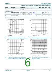
Fig. 2. Continuous drain current as a function of
mounting base temperature
Fig. 1. Normalized total power dissipation as a
function of solder point temperature
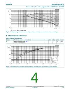
©
PXN012-60QL
All information provided in this document is subject to legal disclaimers.
Nexperia B.V. 2021. All rights reserved
Product data sheet
8 July 2021
3 / 12

 NEXPERIA [ Nexperia ]