Nexperia
PMPB47XP
30 V, single P-channel Trench MOSFET
Symbol
Parameter
Conditions
Min
Typ
-
Max
100
58
Unit
nA
VGS = 12 V; VDS = 0 V; Tj = 25 °C
VGS = -4.5 V; ID = -4 A; Tj = 25 °C
VGS = -4.5 V; ID = -4 A; Tj = 150 °C
VGS = -2.5 V; ID = -3 A; Tj = 25 °C
VGS = -1.8 V; ID = -2.1 A; Tj = 25 °C
VDS = -10 V; ID = -4 A; Tj = 25 °C
-
-
-
-
-
-
RDSon
drain-source on-state
resistance
47
72
54
74
20
mΩ
mΩ
mΩ
mΩ
S
88
71
107
-
gfs
forward
transconductance
RG
gate resistance
f = 1 MHz
-
5.1
-
Ω
Dynamic characteristics
QG(tot)
QGS
QGD
Ciss
total gate charge
VDS = -15 V; ID = -4 A; VGS = -4.5 V;
Tj = 25 °C
-
-
-
-
-
-
14
21
-
nC
nC
nC
pF
pF
pF
gate-source charge
gate-drain charge
input capacitance
output capacitance
2.5
4
-
VDS = -15 V; f = 1 MHz; VGS = 0 V;
Tj = 25 °C
1365
105
90
-
Coss
Crss
-
reverse transfer
capacitance
-
td(on)
tr
td(off)
tf
turn-on delay time
rise time
VDS = -15 V; ID = -4 A; VGS = -4.5 V;
RG(ext) = 6 Ω; Tj = 25 °C
-
-
-
-
15
33
28
20
-
-
-
-
ns
ns
ns
ns
turn-off delay time
fall time
Source-drain diode
VSD source-drain voltage
IS = -1.9 A; VGS = 0 V; Tj = 25 °C
-
-0.7
-1.2
V
017aaa886
017aaa887
-2
-12
-10
-4.5 V
-2 V
I
D
-2.5 V
I
(A)
D
-1.9 V
-1.8 V
-1.7 V
(A)
-3
-4
-5
-6
-10
-8
-4
0
-10
-10
-10
min
typ
max
-1.6 V
V
GS
= -1.5 V
0
-1
-2
-3
-4
0
-0.4
-0.8
-1.2
V
(V)
V
(V)
GS
DS
Tj = 25 °C
Tj = 25 °C; VDS = -5 V
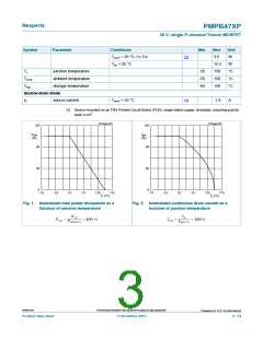
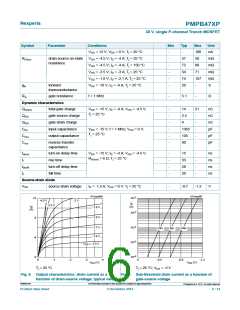
Fig. 6. Output characteristics: drain current as a
function of drain-source voltage; typical values
Fig. 7. Sub-threshold drain current as a function of
gate-source voltage
©
PMPB47XP
All information provided in this document is subject to legal disclaimers.
Nexperia B.V. 2017. All rights reserved
Product data sheet
5 December 2012
6 / 14

 NEXPERIA [ Nexperia ]