Nexperia
PMPB47XP
30 V, single P-channel Trench MOSFET
017aaa892
017aaa893
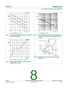
4
3
2
-1.2
10
C
(pF)
V
GS(th)
(V)
C
iss
max
typ
-0.8
-0.4
0
10
C
oss
min
10
C
rss
10
-1
-10
2
-60
0
60
120
180
-1
-10
-10
T (°C)
j
V
(V)
DS
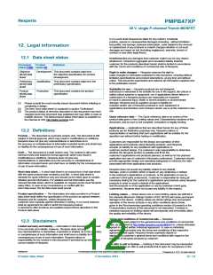
ID = -0.25 mA; VDS = VGS
f = 1 MHz; VGS = 0 V
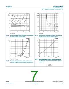
Fig. 12. Gate-source threshold voltage as a function of Fig. 13. Input, output and reverse transfer capacitances
junction temperature
as a function of drain-source voltage; typical
values
017aaa894
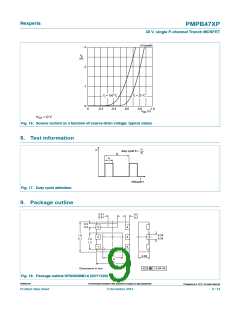
-4.5
GS
V
DS
V
I
D
(V)
-3.0
V
GS(pl)
V
GS(th)
GS
V
-1.5
Q
GS1
Q
GS2
Q
Q
GD
GS
Q
G(tot)
017aaa137
0
Fig. 15. MOSFET transistor: Gate charge waveform
definitions
0
3
6
9
12
Q
15
(nC)
G
ID = -3 A; VDS = -15 V; Tamb = 25 °C
Fig. 14. Gate-source voltage as a function of gate
charge; typical values
©
PMPB47XP
All information provided in this document is subject to legal disclaimers.
Nexperia B.V. 2017. All rights reserved
Product data sheet
5 December 2012
8 / 14

 NEXPERIA [ Nexperia ]