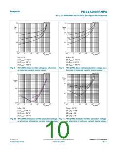
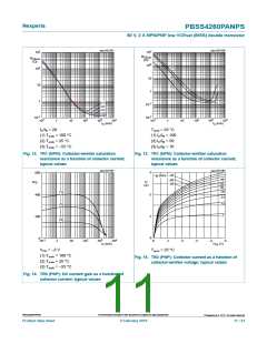
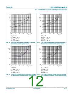
Nexperia
PBSS4260PANPS
60 V, 2 A NPN/PNP low VCEsat (BISS) double transistor
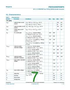
Symbol
Parameter
Conditions
Min
Typ
90
Max
Unit
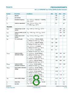
ns
ton
ts
turn-on time
storage time
fall time
-
-
-
-
-
-
-
-
-
-
195
75
ns
tf
ns
toff
fT
turn-off time
transition frequency
270
100
ns
VCE = -10 V; IC = -500 mA;
f = 100 MHz; Tamb = 25 °C
MHz
Cc
collector capacitance
VCB = -10 V; IE = 0 A; ie = 0 A;
f = 1 MHz; Tamb = 25 °C
-
16
-
pF
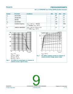
aaa-021199
aaa-021200
800
3
I
(mA) = 55.0
49.5
B
(1)
(2)
44.0
38.5
h
FE
I
C
33.0
27.5
22.0
(A)
600
2
1
0
16.5
11.0
400
200
0
(3)
5.5
-1
2
3
4
10
1
10
10
10
10
(mA)
0
1
2
3
4
5
I
V
(V)
CE
C
VCE = 2 V
Tamb = 25 °C
(1) Tamb = 100 °C
(2) Tamb = 25 °C
(3) Tamb = −55 °C
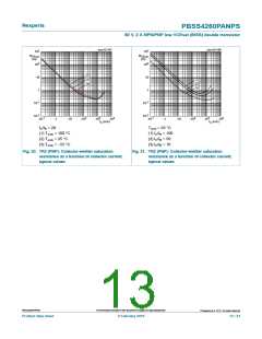
Fig. 7. TR1 (NPN): Collector current as a function of
collector-emitter voltage; typical values
Fig. 6. TR1 (NPN): DC current gain as a function of
collector current; typical values
©
PBSS4260PANPS
All information provided in this document is subject to legal disclaimers.
Nexperia B.V. 2017. All rights reserved
Product data sheet
4 February 2016
9 / 21

 NEXPERIA [ Nexperia ]