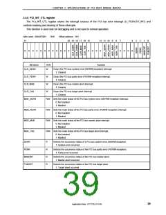
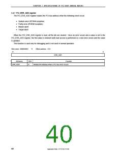
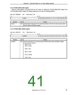
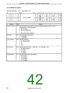
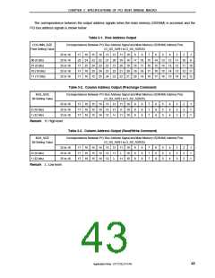
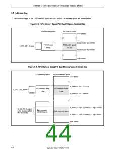
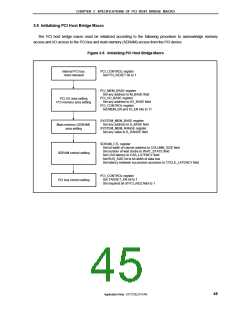
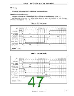
CHAPTER 3 SPECIFICATIONS OF PCI HOST BRIDGE MACRO
The correspondence between the output address signals when the main memory (SDRAM) is accessed and the
PCI bus address signals is shown below.
Table 3-1. Row Address Output
COLUMN_SIZE
Correspondence Between PCI Bus Address Signal and Main Memory (SDRAM) Address Pins
(O_SD_ADR1 to O_SD_ADR25)
Field Setting Value
25 to 18
25 to 18
25 to 18
25 to 18
25 to 18
17 16 15 14 13 12 11 10
9
8
7
6
5
4
3
2
1
9
00 (8 bits)
01 (9 bits)
10 (10 bits)
11 (11 bits)
25 24 23 22 21 20 19 18 17 16 15 14 13 12 11 10
17 25 24 23 22 21 20 19 18 17 16 15 14 13 12 11 10
17 16 25 24 23 22 21 20 19 18 17 16 15 14 13 12 11
17 16 15 25 24 23 22 21 20 19 18 17 16 15 14 13 12
Table 3-2. Column Address Output (Precharge Command)
BUS_SIZE
Correspondence Between PCI Bus Address Signal and Main Memory (SDRAM) Address Pins
(O_SD_ADR1 to O_SD_ADR25)
Bit Setting Value
25 to 18
25 to 18
25 to 18
17 16 15 14 13 12 11 10
17 16 15 14 12 11 10
17 16 15 14 12 11 10
9
9
9
8
8
8
7
7
7
6
6
6
5
5
5
4
4
4
3
3
3
2
2
2
1
1
1
0 (16 bits)
1 (32 bits)
H
H
Remark H: High level
Table 3-3. Column Address Output (Read/Write Command)
BUS_SIZE
Correspondence Between PCI Bus Address Signal and Main Memory (SDRAM) Address Pins
(O_SD_ADR1 to O_SD_ADR25)
Bit Setting Value
25 to 18
17 16 15 14 13 12 11 10
17 16 15 14 12 11 10
17 16 15 14 12 11 10
9
9
9
8
8
8
7
7
7
6
6
6
5
5
5
4
4
4
3
3
3
2
2
2
1
1
1
0 (16 bits)
1 (32 bits)
25 to 18
25 to 18
L
L
Remark L: Low level
43
Application Note U17121EJ1V1AN

 NEC [ NEC ]