CHAPTER 3 SPECIFICATIONS OF PCI HOST BRIDGE MACRO
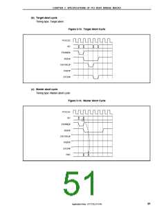
3.8 Timing
The timing for each interface of the PCI host bridge macro is shown below.
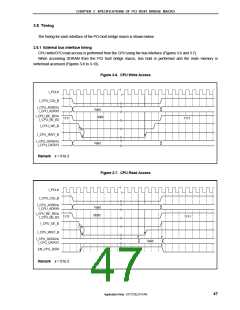
3.8.1 External bus interface timing
CPU write/CPU read access is performed from the CPU using the bus interface (Figures 3-6 and 3-7).
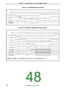
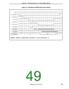
When accessing SDRAM from the PCI host bridge macro, bus hold is performed and the main memory is
write/read accessed (Figures 3-8 to 3-10).
Figure 3-6. CPU Write Access
I_PCLK
I_CPU_CSx_B
I_CPU_ADR0 to
Valid
I_CPU_ADR19
I_CPU_BE_B0 to
0000
1111
1111
I_CPU_BE_B3
I_CPU_WE_B
I_CPU_WAIT_B
I_CPU_DATA0 to
I_CPU_DATA31
Valid
Remark x = 0 to 2
Figure 3-7. CPU Read Access
I_PCLK
I_CPU_CSx_B
I_CPU_ADR0 to
I_CPU_ADR19
Valid
0000
I_CPU_BE_B0 to
I_CPU_BE_B3
1111
1111
I_CPU_OE_B
I_CPU_WAIT_B
I_CPU_DATA0 to
I_CPU_DATA31
Valid
EN_CPU_DATA
Remark x = 0 to 2
47
Application Note U17121EJ1V1AN

 NEC [ NEC ]