µPD703100A-33, 703100A-40, 703101A-33, 703102A-33
16. ELECTRICAL SPECIFICATIONS (PRELIMINARY VALUES)
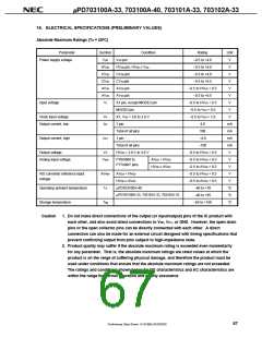
Absolute Maximum Ratings (TA = 25°C)
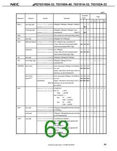
Parameter
Symbol
Condition
Rating
−0.5 to +4.6
−0.5 to +4.6
−0.5 to +4.6
−0.5 to +0.5
−0.5 to HVDD + 0.5
−0.5 to +0.5
−0.5 to HVDD + 0.5
−0.5 to VDD + 0.5
−0.5 to VDD + 1.0
4.0
Unit
V
Power supply voltage
VDD
HVDD
CVDD
CVSS
AVDD
AVSS
VI
VDD pin
HVDD pin, HVDD ≥ VDD
CVDD pin
V
V
CVSS pin
V
AVDD pin
V
AVSS pin
V
Input voltage
X1 pin, except MODE3 pin
MODE3 pin
V
V
Clock input voltage
Output current, low
VK
IOL
X1, VDD = 3.0 to 3.6 V
1 pin
V
mA
mA
mA
mA
V
Total of all pins
1 pin
100
Output current, high
IOH
−4.0
Total of all pins
HVDD = 3.0 V to 3.6 V
−100
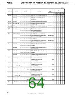
Output voltage
VO
−0.5 to HVDD + 0.5
−0.5 to HVDD + 0.5
−0.5 to AVDD + 0.5
−0.5 to HVDD + 0.5
−0.5 to AVDD + 0.5
−40 to +70
Analog input voltage
VIAN
P70/ANI0 to
AVDD > HVDD
V
P77/ANI7 pins
HVDD ≥ AVDD
V
A/D converter reference input
voltage
AVREF
AVDD > HVDD
HVDD ≥ AVDD
V
V
Operating ambient temperature
Storage temperature
TA
µPD703100A-40
°C
°C
°C
µ
PD703100A-33, 703101A-33, 703102A-33
−40 to +85
Tstg
−65 to +150
Caution
1. Do not make direct connections of the output (or input/output) pins of the IC product with
each other, and also avoid direct connections to VDD, VCC, or GND. However, the open drain
pins or the open collector pins can be directly connected with each other. A direct
connection can also be made for an external circuit designed with timing specifications that
prevent conflicting output from pins subject to high-impedance state.
2. Product quality may suffer if the absolute maximum rating is exceeded even momentarily
for any parameter. That is, the absolute maximum ratings are rated values at which the
product is on the verge of suffering physical damage, and therefore the product must be
used under conditions that ensure that the absolute maximum ratings are not exceeded.
The ratings and conditions shown below for DC characteristics and AC characteristics are
within the range for normal operation and quality assurance.
67
Preliminary Data Sheet U14168EJ2V0DS00

 NEC [ NEC ]