µPD703100A-33, 703100A-40, 703101A-33, 703102A-33
(7/7)
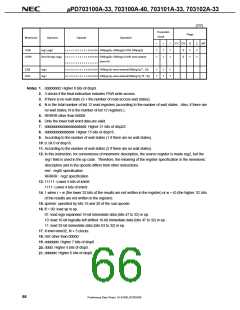
Execution
Flags
Clock
Mnemonic
Operand
Opcode
Operation
i
r
l
CY OV
S
×
×
Z
×
×
SAT
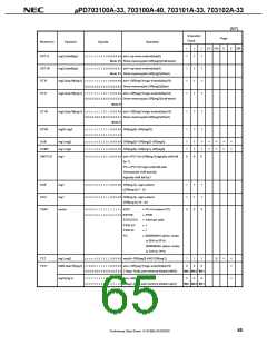
XOR
reg1,reg2
rr r r r 0 0 1 0 0 1 R R R R R GR[reg2]←GR[reg2] XOR GR[reg1]
1
1
1
1
1
1
0
0
XORI
imm16,reg1,reg2 rr r r r 1 1 0 1 0 1 R R R R R GR[reg2]←GR[reg1] XOR zero-extend
(imm16)
ii i i i i i i i i i i i i i i
ZXB
ZXH
reg1
reg1
00 0 0 0 0 0 0 1 0 0 R R R R R GR[reg1]←zero-extend(GR[reg1] (7 : 0))
00 0 0 0 0 0 0 1 1 0 R R R R R GR[reg1]←zero-extend(GR[reg1] (15 : 0))
1
1
1
1
1
1
Notes 1. dddddddd: Higher 8 bits of disp9.
2. 3 clocks if the final instruction includes PSW write access.
3. If there is no wait state (3 + the number of read access wait states).
4. N is the total number of list 12 read registers (according to the number of wait states. Also, if there are
no wait states, N is the number of list 12 registers.).
5. RRRRR other than 00000.
6. Only the lower half word data are valid.
7. ddddddddddddddddddddd: Higher 21 bits of disp22.
8. ddddddddddddddd: Higher 15 bits of disp16.
9. According to the number of wait states (1 if there are no wait states).
10. b: bit 0 of disp16.
11. According to the number of wait states (2 if there are no wait states).
12. In this instruction, for convenience of mnemonic description, the source register is made reg2, but the
reg1 field is used in the op code. Therefore, the meaning of the register specification in the mnemonic
description and in the opcode differs from other instructions.
rrrrr: regID specification
RRRRR: reg2 specification
13. 11111: Lower 5 bits of imm9.
1111: Lower 4 bits of imm9.
14. 1 when r = w (the lower 32 bits of the results are not written in the register) or w = r0 (the higher 32 bits
of the results are not written in the register).
15. sp/imm: specified by bits 19 and 20 of the sub opcode.
16. ff = 00: load sp in ep.
01: load sign expanded 16-bit immediate data (bits 47 to 32) in ep.
10: load 16-bit logically left shifted 16-bit immediate data (bits 47 to 32) in ep.
11: load 32-bit immediate data (bits 63 to 32) in ep.
17. If imm=imm32, N + 3 clocks.
18. rrrrr other than 00000.
19. ddddddd: Higher 7 bits of disp8.
20. dddd: Higher 4 bits of disp5.
21. dddddd: Higher 6 bits of disp8.
66
Preliminary Data Sheet U14168EJ2V0DS00

 NEC [ NEC ]