µPD703100A-33, 703100A-40, 703101A-33, 703102A-33
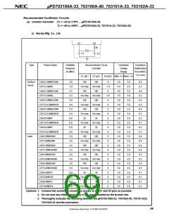
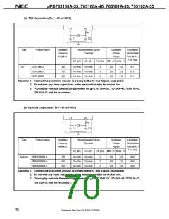
(ii) TDK Corporation (TA = –40 to +85°C)
X1
X2
Rd
C1
C2
Type
Product Name
Oscillation
Frequency
Recommended Circuit
Constant
Oscillation
Voltage
Range
Oscillation
Stabilization
Time (MAX.)
TOST (ms)
f
XX (MHz)
C1 (pF)
C2 (pF)
Rd (kΩ) MIN. (V) MAX. (V)
TDK
CCR4.0MC3
4.0
5.0
8.0
On-chip
On-chip
On-chip
On-chip
On-chip
On-chip
0
0
0
3.0
3.0
3.0
3.6
3.6
3.6
0.17
0.15
0.11
CCR5.0MC3
CCR8.0MC5
Cautions 1. Connect the oscillation circuits as closely to the X1 and X2 pins as possible.
2. Do not wire any other signal lines in the area indicated by the broken line.
3. Thoroughly evaluate the matching between the µPD703100A-33, 703100A-40, 703101A-33,
703102A-33 and the resonators.
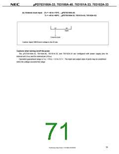
(iii) Kyocera Corporation (TA = –20 to +80°C)
X1
X2
Rd
C1
C2
Type
Product Name
Oscillation
Frequency
Recommended Circuit
Constant
Oscillation
Voltage
Range
Oscillation
Stabilization
Time (MAX.)
TOST (ms)
f
XX (MHz)
C1 (pF)
C2 (pF)
Rd (kΩ) MIN. (V) MAX. (V)
Kyocera
PBRC5.00BR-A
PBRC6.00BR-A
PBRC6.60BR-A
5.0
6.0
6.6
On-chip
On-chip
On-chip
On-chip
On-chip
On-chip
0
0
0
3.0
3.0
3.0
3.6
3.6
3.6
0.06
0.06
0.06
Cautions 1. Connect the oscillation circuits as closely to the X1 and X2 pins as possible.
2. Do not wire any other signal lines in the area indicated by the broken line.
3. Thoroughly evaluate the matching between the µPD703100A-33, 703100A-40, 703101A-33,
703102A-33 and the resonators.
70
Preliminary Data Sheet U14168EJ2V0DS00

 NEC [ NEC ]