µPD703100A-33, 703100A-40, 703101A-33, 703102A-33
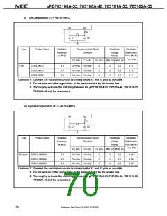
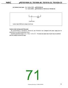
(b) External clock input (TA = –40 to +70°C ... µPD703100A-40,
TA = –40 to +85°C ... µPD703100A-33, 703101A-33, 703102A-33)
X1
X2
Open
External clock
Caution Input CMOS-level voltage to the X1 pin.
Cautions when turning on/off the power
The µPD703100A-33, 703100A-40, 703101A-33, and 703102A-33 are configured with power supply pins for
internal unit (VDD) and for external pin (HVDD).
Operation guaranteed range is VDD = HVDD = 3.0 to 3.6 V. The input and output state of ports may be undefined
when the voltage exceeds this range.
71
Preliminary Data Sheet U14168EJ2V0DS00

 NEC [ NEC ]