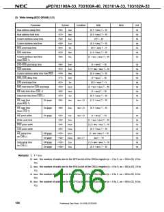
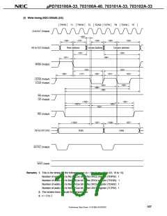
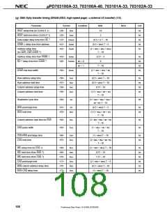
µPD703100A-33, 703100A-40, 703101A-33, 703102A-33
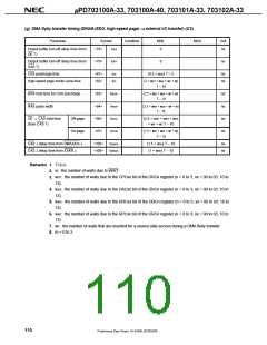
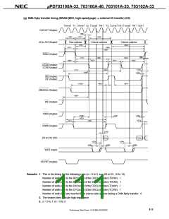
(g) DMA flyby transfer timing (DRAM (EDO, high-speed page) → external I/O transfer) (2/3)
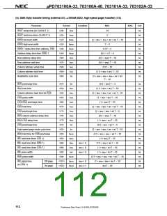
Parameter
Symbol
<78> tOEZ
Condition
MIN.
0
MAX.
Unit
ns
Output buffer turn-off delay time (from
OE ↑)
Output buffer turn-off delay time (from
<79>
tOFF
0
ns
CAS ↑)
CAS precharge time
<81>
<82>
tCP
tPC
(0.5 + wCP) T – 5
ns
ns
High-speed page mode cycle time
(2 + wCP + wDA + w
F
+ w)
T – 10
RAS hold time for CAS precharge
RAS pulse width
<83>
<94>
<96>
<97>
tRHCP
tRASP
tOCH1
tOCH2
(2.5 + wCP + wDA + w
F
+ w)
ns
ns
ns
ns
T – 10
(2.5 + wRH + wDA + w
T – 10
F
+ w)
OE → CAS hold time
(from CAS ↑)
Off-page
On-page
(2.5 + wRP + wRH + wDA
+ wF + w) T – 10
(1.5 + wCP + wDA + w
F
+ w)
T – 10
CAS ↓ delay time from DMAAKm ↓
CAS ↓ delay time from IOWR ↓
<105>
<106>
tDDACS
tDRDCS
(1.5 + wRH) T – 10
(1 + wRH) T – 10
ns
ns
Remarks 1. T=tCYK
2. w: the number of waits due to WAIT.
3. wCP: the number of waits due to the CPCxx bit of the DRCn register (n = 0 to 3, xx = 00 to 03, 10 to
13).
4. wDA: the number of waits due to the DACxx bit of the DRCn register (n = 0 to 3, xx = 00 to 03, 10 to
13).
5. wRH: the number of waits due to the RHCxx bit of the DRCn register (n = 0 to 3, xx = 00 to 03, 10 to
13).
6. wRP: the number of waits due to the RPCxx bit of the DRCn register (n = 0 to 3, xx = 00 to 03, 10 to
13).
7. wF: the number of waits that are inserted for a source-side access during a DMA flyby transfer.
8. m = 0 to 3
110
Preliminary Data Sheet U14168EJ2V0DS00

 NEC [ NEC ]