µPD703100A-33, 703100A-40, 703101A-33, 703102A-33
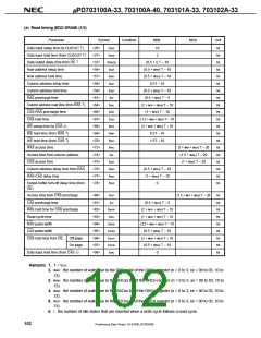
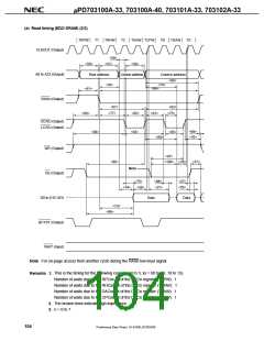
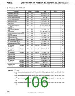
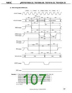
(f) Write timing (EDO DRAM) (1/2)
Parameter
Row address setup time
Row address hold time
Column address setup time
Column address hold time
RAS precharge time
Symbol
<56>
Condition
MIN.
MAX.
Unit
ns
ns
ns
ns
ns
ns
ns
tASR
tRAH
tASC
tCAH
tRP
(0.5 + wRP) T – 10
(0.5 + wRH) T – 10
0.5T – 10
<57>
<58>
<59>
<61>
<63>
<64>
(0.5 + wDA) T – 10
(0.5 + wRP) T – 5
(1.5 + wDA) T – 10
(2 + wCP + wDA) T – 10
RAS hold time
tRSH
tRAL
Column address read time
(from RAS ↑)
CAS-RAS precharge time
CAS hold time
<66>
<67>
<76>
<77>
<81>
<83>
<85>
<87>
<88>
tCRP
tCSH
tRAD
tRCD
tCP
(1 + wRP) T – 10
ns
ns
ns
ns
ns
ns
ns
ns
ns
(1.5 + wRH + wDA) T – 10
Column address delay time from RAS
RAS-CAS delay time
(0.5 + wRH) T – 10
(1 + wRH) T – 10
CAS precharge time
(0.5 + wCP) T – 5
(2 + wCP + wDA) T – 10
(1 + wDA) T – 10
RAS hold time for CAS precharge
WE hold time (from CAS ↓)
Data hold time (from CAS ↓)
tRHCP
tWCH
tDH
(0.5 + wDA) T – 10
(1.5 + wDA) T – 10
WE read time
On-page
On-page
On-page
tRWL
wCP = 0
wCP = 0
wCP = 0
(from RAS ↑)
WE read time
<89>
tCWL
(0.5 + wDA) T – 10
ns
(from CAS ↑)
WE pulse width
Write cycle time
RAS pulse width
CAS pulse width
<92>
<93>
tWP
tHPC
(1 + wDA) T – 10
ns
ns
ns
ns
ns
ns
ns
ns
(1 + wDA + wCP) T – 10
<94>
tRASP
tHCAS
tWCS1
tWCS2
tDS1
(2.5 + wRH + wDA
)
T – 10
(0.5 + wDA) T – 10
T – 10
wCPT – 10
T – 10
(0.5 + wCP) T – 10
<95>
WE setup time
Off-page
On-page
Off-page
On-page
<101>
<102>
<103>
<104>
(1 + wRP + wRH
)
(to CAS ↓)
wCP ≥ 1
Data setup time
(1.5 + wRP + wRH
)
(to CAS ↓)
tDS2
Remarks 1. T = tCYK
2. wRP: the number of waits due to the RPCxx bit of the DRCn register (n = 0 to 3, xx = 00 to 03, 10 to
13).
3. wRH: the number of waits due to the RHCxx bit of the DRCn register (n = 0 to 3, xx = 00 to 03, 10 to
13).
4. wDA: the number of waits due to the DACxx bit of the DRCn register (n = 0 to 3, xx = 00 to 03, 10 to
13).
5. wCP: the number of waits due to the CPCxx bit of the DRCn register (n = 0 to 3, xx = 00 to 03, 10 to
13).
106
Preliminary Data Sheet U14168EJ2V0DS00

 NEC [ NEC ]