µPD703100A-33, 703100A-40, 703101A-33, 703102A-33
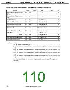
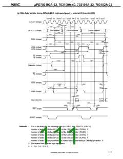
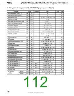
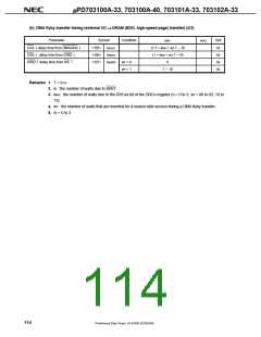
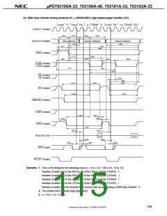
Remarks 1. T = tCYK
2. w: the number of waits due to WAIT.
3. wRH: the number of waits due to the RHCxx bit of the DRCn register (n = 0 to 3, xx = 00 to 03, 10 to
13).
4. wDA: the number of waits due to the DACxx bit of the DRCn register (n = 0 to 3, xx = 00 to 03, 10 to
13).
5. wRP: the number of waits due to the RPCxx bit of the DRCn register (n = 0 to 3, xx = 00 to 03, 10 to
13).
6. wCP: the number of waits due to the CPCxx bit of the DRCn register (n = 0 to 3, xx = 00 to 03, 10 to
13).
7. wF: the number of waits that are inserted for a source-side access during a DMA flyby transfer.
8. i: the number of idle states that are inserted when a write cycle follows a read cycle.
9. n = 0 to 7
113
Preliminary Data Sheet U14168EJ2V0DS00

 NEC [ NEC ]