Index
out of page
read access 2-23
A
wait states selection guide 2-20
write access 2-24
ac electrical characteristics 2-4
address bus 1-1
Page mode
Address Trace mode 2-25, 2-27
applications iv
arbitration bus timings 2-27
read accesses 2-19
wait states selection guide 2-16
write accesses 2-19
B
refresh access 2-24
DSP56300
Family Manual iv
DSP56303
benchmark test algorithm A-1
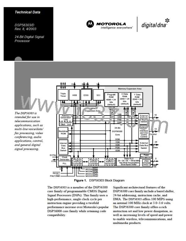
block diagram i
bootstrap ROM iii
Boundary Scan (JTAG Port) timing diagram 2-46
bus
block diagram i
Technical Data iv
User’s Manual iv
acquisition timings 2-28
address 1-2
control 1-1
E
electrical
design considerations 4-2, 4-3
data 1-2
external address 1-5
external data 1-5
multiplexed 1-2
non-multiplexed 1-2
release timings 2-28, 2-29
Enhanced Synchronous Serial Interface (ESSI) iii,
1-1, 1-2, 1-13, 1-14
receiver timing 2-42
transmitter timing 2-41
external address bus 1-5
C
external bus control 1-5, 1-6, 1-7
external bus synchronous timings (SRAM
access) 2-25
external clock operation 2-4
external data bus 1-5
clock 1-1, 1-4
external 2-4
clocks
internal 2-4
external interrupt timing (negative
edge-triggered) 2-11
crystal oscillator circuits 2-5
external level-sensitive fast interrupt timing 2-10
external memory access (DMA Source)
timing 2-12
External Memory Expansion Port 2-13
external memory expansion port 1-5
D
data bus 1-1
data memory expansion iv
Data Strobe (DS) 1-2
dc electrical characteristics 2-3
DE signal 1-18
F
Debug Event signal (DE signal) 1-18
Debug mode
functional groups 1-2
functional signal groups 1-1
entering 1-18
external indication 1-18
Debug support iii
design considerations
electrical 4-2, 4-3
PLL 4-5
G
General-Purpose Input/Output (GPIO) iii, 1-2
ground 1-1, 1-3
PLL 1-3
power consumption 4-4
thermal 4-1
H
documentation list iv
Double Data Strobe 1-2
DRAM
Host Interface (HI08) iii, 1-1, 1-2, 1-9, 1-10,
1-11, 1-12
controller iv
Index-1

 MOTOROLA [ MOTOROLA ]