MITSUBISHI MICROCOMPUTERS
3827 Group
SINGLE-CHIP 8-BIT CMOS MICROCOMPUTER
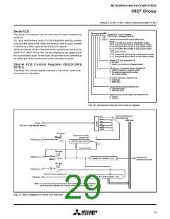
Serial I/O2
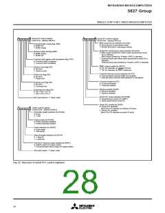
b7
b0
Serial I/O2 control register
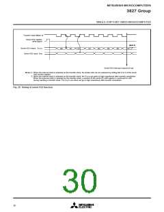
The serial I/O2 function can be used only for clock synchronous
(SIO2CON : address 001D16)
serial I/O.
Internal synchronous clock select bits
b2 b1 b0
0 0 0: f(XIN)/8 (f(XCIN)/8 in low-speed mode)
For clock synchronous serial I/O2 the transmitter and the receiver
must use the same clock. When the internal clock is used, transfer
is started by a write signal to the serial I/O2 register.
When an internal clock is selected as the synchronous clock of the
serial I/O2, either P62 or P63 can be selected as an output pin of
the synchronous clock. In this case, the pin that is not selected as
an output pin of the synchronous clock functions as a port.
0 0 1: f(XIN)/16 (f(XCIN)/16 in low-speed mode)
0 1 0: f(XIN)/32 (f(XCIN)/32 in low-speed mode)
0 1 1: f(XIN)/64 (f(XCIN)/64 in low-speed mode)
1 0 0:
Do not set
1 0 1:
1 1 0: f(XIN)/128 (f(XCIN)/128 in low-speed mode)
1 1 1: f(XIN)/256 (f(XCIN)/256 in low-speed mode)
Serial I/O2 port selection bit
0: I/O port
1: SOUT2,SCLK21/SCLK22 signal output
[Serial I/O2 Control Register (SIO2CON)]
001D16
P61/SOUT2 P-channel output disable bit
0: CMOS output (in output mode)
1: N-channel open-drain output
(in output mode)
The serial I/O2 control register contains 8 bits which control vari-
ous serial I/O2 functions.
Transfer direction selection bit
0: LSB first
1: MSB first
Synchronous clock selection bit
0: External clock
1: Internal clock
Synchronous clock output pin selection bit
0: SCLK21
1: SCLK22
Fig. 26 Structure of serial I/O2 control register
Internal synchronous
clock select bits
1/8
1/16
Data bus
1/32
f(XIN
)
1/64
(f(XCIN) in low-speed mode)
1/128
1/256
P63 latch
Synchronous clock
selection bit
(Note)
“1”
P6
3
/SCLK22
Synchronous circuit
“0”
External clock
P62 latch
“0”
P6
P6
2
1
/SCLK21
/SOUT2
Serial I/O2
interrupt request
Serial I/O counter 2 (3)
(Note)
“1”
P61
latch
“0”
“1”
Serial I/O2 port selection bit
Serial I/O shift register 2 (8)
P60/SIN2
Note: It is selected by the synchronous clock selection bit, the synchronous
clock output pin selection bit, and the serial I/O port selection bit.
Fig. 27 Block diagram of serial I/O2 function
29

 MITSUBISHI [ Mitsubishi Group ]