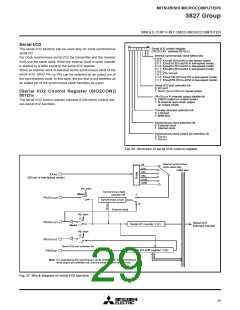
MITSUBISHI MICROCOMPUTERS
3827 Group
SINGLE-CHIP 8-BIT CMOS MICROCOMPUTER
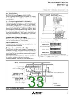
A-D CONVERTER
b7
b0
A-D control register
(ADCON : address 003116)
[A-D Conversion Register (AD)] 003516
The A-D conversion register is a read-only register that contains
the result of an A-D conversion. During A-D conversion, do not
read this register.
Analog input pin selection bits
0 0 0 : P60/SIN2/AN0
0 0 1 : P61/SOUT2/AN1
0 1 0 : P62/SCLK21/AN2
0 1 1 : P63/SCLK22/AN3
1 0 0 : P64/AN4
[A-D Control Register (ADCON)] 003416
The A-D control register controls the A-D conversion process. Bits
0 to 2 are analog input pin selection bits. Bit 3 is an A-D conver-
sion completion bit and “0” during A-D conversion, then changes
to “1” when the A-D conversion is completed. Writing “0” to this bit
starts the A-D conversion. Bit 4 controls the transistor which
breaks the through current of the resistor ladder. When bit 5, which
is the AD external trigger valid bit, is set to “1”, A-D conversion is
started even by a rising edge or falling edge of an ADT input. Set
ports which share with ADT pins to input when using an A-D exter-
nal trigger.
1 0 1 : P65/AN5
1 1 0 : P66/AN6
1 1 1 : P67/AN7
AD conversion completion bit
0 : Conversion in progress
1 : Conversion completed
VREF input switch bit
0 : OFF
1 : ON
AD external trigger valid bit
0 : A-D external trigger invalid
1 : A-D external trigger valid
Interrupt source selection bit
0 : Interrupt request at A-D
conversion completed
1 : Interrupt request at ADT
input rising or falling
Reference voltage input selection bit
0 : VREF
[Comparison Voltage Generator]
The comparison voltage generator divides the voltage between
1 : P56/DA1
AVSS and VREF, and outputs the divided voltages.
8-bit read (Read only address 003216.)
b7
[Channel Selector]
The channel selector selects one of the input ports P67/AN7–P60/
b0
(Address 003216)
b9 b8 b7 b6 b5 b4 b3 b2
AN0, and inputs it to the comparator.
10-bit read (Read address 003316 first.)
b7
b0
[Comparator and Control Circuit]
(Address 003316)
b9 b8
The comparator and control circuit compares an analog input volt-
age with the comparison voltage and stores the result in the A-D
conversion register. When an A-D conversion is completed, the
control circuit sets the AD conversion completion bit and the AD
interrupt request bit to “1”.
b7
b0
(Address 003216)
b7 b6 b5 b4 b3 b2 b1 b0
Note: High-order 6 bits of address 003316 becomes “0” at reading.
Note that the comparator is constructed linked to a capacitor, so
set f(XIN) to at least 500 kHz during A-D conversion.
Fig. 33 Structure of A-D control register
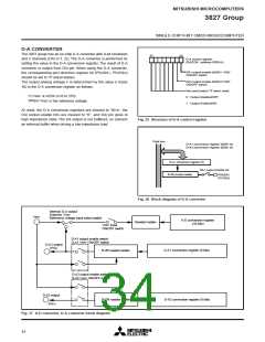
Use a clock divided the main clock XIN as the internal clock φ.
Data bus
b0
b7
A-D control register
P40/ADT
3
A-D control register
ADT/A-D interrupt request
P60/SIN2/AN0
P61/SOUT2/AN1
(L)
(H)
P62/SCLK21/AN2
Comparater
A-D conversion register A-D conversion register
P63/SCLK22/AN3
10
P64/AN4
Resistor ladder
AVSS
P65/AN5
P66/AN6
P67/AN7
VREF
P56/DA1
Fig. 34 A-D converter block diagram
33

 MITSUBISHI [ Mitsubishi Group ]