Mitsubishi microcomputers
M16C / 62 Group
SINGLE-CHIP 16-BIT CMOS MICROCOMPUTER
CPU Rewrite Mode (Flash Memory Version)
Bit 3 of the flash memory control register 1 turns power supply to the internal flash memory on/off. When
this bit is set to “1”, power is not supplied to the internal flash memory, thus power consumption can be
reduced. However, in this state, the internal flash memory cannot be accessed. To set this bit to “1”, it is
necessary to write “0” and then write “1” in succession. Use this bit mainly in the low speed mode (when
XCIN is the block count source of BCLK).
When the CPU is shifted to the stop or wait modes, power to the internal flash memory is automatically shut
off. It is reconnected automatically when CPU operation is restored. Therefore, it is not particularly neces-
sary to set flash memory control register 1.
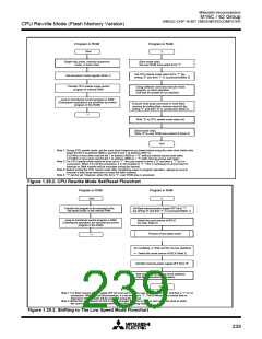
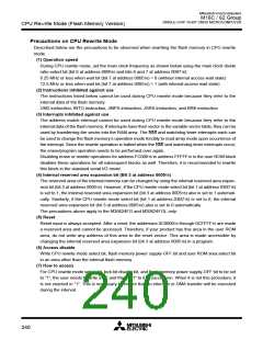
Figure 1.29.2 shows a flowchart for setting/releasing the CPU rewrite mode. Figure 1.29.3 shows a flow-
chart for shifting to the low speed mode. Always perform operation as indicated in these flowcharts.
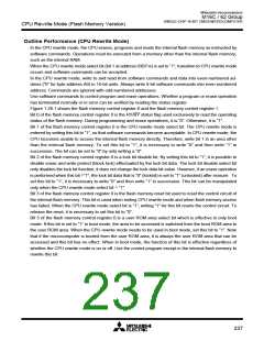
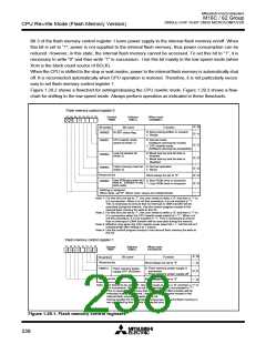
Flash memory control register 0
b7 b6 b5 b4 b3 b2 b1 b0
Symbol
FMR0
Address
03B716
When reset
XX000001
2
0
R
W
Bit name
Function
Bit symbol
FMR00
R W
0: Busy (being written or erased)
1: Ready
RY/BY status flag
CPU rewrite mode
select bit (Note 1)
0: Normal mode
(Software commands invalid)
1: CPU rewrite mode
FMR01
(Software commands acceptable)
Lock bit disable bit
(Note 2)
0: Block lock by lock bit data is
enabled
1: Block lock by lock bit data is
disabled
FMR02
FMR03
Flash memory reset bit 0: Normal operation
(Note 3)
1: Reset
Reserved bit
User ROM area select bit (
Must always be set to “0”
0: Boot ROM area is accessed
1: User ROM area is accessed
FMR05
Note 4) (Effective in only
boot mode)
Nothing is assigned.
When write, set "0". When read, values are indeterminate.
Note 1: For this bit to be set to “1”, the user needs to write a “0” and then a “1” to
it in succession. When it is not this procedure, it is not enacted in “1”.
This is necessary to ensure that no interrupt or DMA transfer will be
executed during the interval. Use the control program except in the
internal flash memory for write to this bit.
Note 2: For this bit to be set to “1”, the user needs to write a “0” and then a “1” to
it in succession when the CPU rewrite mode select bit = “1”. When it is
not this procedure, it is not enacted in “1”. This is necessary to ensure
that no interrupt or DMA transfer will be executed during the interval.
Note 3: Effective only when the CPU rewrite mode select bit = 1. Set this bit to 0
subsequently after setting it to 1 (reset).
Note 4: Use the control program except in the internal flash memory for write to
this bit.
Flash memory control register 1
b7 b6 b5 b4 b3 b2 b1 b0
Symbol
FMR1
Address
03B616
When reset
XXXX0XXX
2
0
0
0
0
0 0 0
R
W
Bit name
Function
Bit symbol
R W
Reserved bit
Must always be set to “0”
0: Flash memory power supply is
connected
1: Flash memory power supply-off
FMR13
Flash memory power
supply-OFF bit (Note)
Reserved bit
Must always be set to “0”
Note : For this bit to be set to “1”, the user needs to write a “0” and then a “1” to
it in succession. When it is not this procedure, it is not enacted in “1”.
This is necessary to ensure that no interrupt or DMA transfer will be
executed during the interval. Use the control program except in the
internal flash memory for write to this bit.
During parallel I/O mode,programming,erase or read of flash memory is
not controlled by this bit,only by external pins.
Figure 1.29.1. Flash memory control registers
238

 MITSUBISHI [ Mitsubishi Group ]