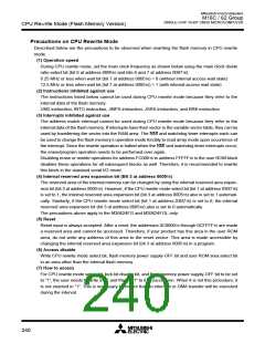
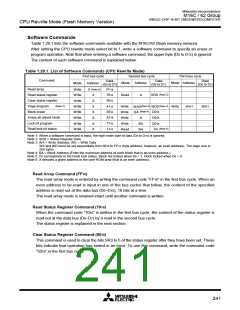
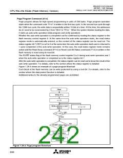
Mitsubishi microcomputers
M16C / 62 Group
SINGLE-CHIP 16-BIT CMOS MICROCOMPUTER
CPU Rewrite Mode (Flash Memory Version)
Precautions on CPU Rewrite Mode
Described below are the precautions to be observed when rewriting the flash memory in CPU rewrite
mode.
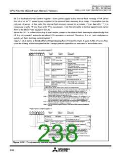
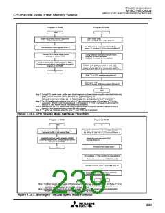
(1) Operation speed
During CPU rewrite mode, set the main clock frequency as shown below using the main clock divide
ratio select bit (bit 6 at address 000616 and bits 6 and 7 at address 000716):
6.25 MHz or less when wait bit (bit 7 at address 000516) = 0 (without internal access wait state)
12.5 MHz or less when wait bit (bit 7 at address 000516) = 1 (with internal access wait state)
(2) Instructions inhibited against use
The instructions listed below cannot be used during CPU rewrite mode because they refer to the
internal data of the flash memory:
UND instruction, INTO instruction, JMPS instruction, JSRS instruction, and BRK instruction
(3) Interrupts inhibited against use
The address match interrupt cannot be used during CPU rewrite mode because they refer to the
internal data of the flash memory. If interrupts have their vector in the variable vector table, they can be
_______
used by transferring the vector into the RAM area. The NMI and watchdog timer interrupts each can
be used to change the flash memory’s operation mode forcibly to read array mode upon occurrence of
_______
the interrupt. Since the rewrite operation is halted when the NMI and watchdog timer interrupts occur,
the erase/program operation needs to be performed over again.
Disabling erase or rewrite operations for address FC00016 to address FFFFF16 in the user ROM block
disables these operations for all subsequent blocks as well. Therefore, it is recommended to rewrite
this block in the standard serial I/O mode.
(4) Internal reserved area expansion bit (Bit 3 at address 000516)
The reserved area of the internal memory can be changed by using the internal reserved area expan-
sion bit (bit 3 at address 000516). However, if the CPU rewrite mode select bit (bit 1 at address 03B716)
is set to 1, the internal reserved area expansion bit (bit 3 at address 000516) also is set to 1 automati-
cally. Similarly, if the CPU rewrite mode select bit (bit 1 at address 03B716) is set to 0, the internal
reserved area expansion bit (bit 3 at address 000516) also is set to 0 automatically.
The precautions above apply to the M30624FG and M30624FGL only.
(5) Reset
Reset input is always accepted. After a reset, the addresses 0C000016 through 0CFFFF16 are made
a reserved area and cannot be accessed. Therefore, if your product has this area in the user ROM
area, do not write any address of this area to the reset vector. This area is made accessible by
changing the internal reserved area expansion bit (bit 3 at address 000516) in a program.
(6) Access disable
Write CPU rewrite mode select bit, flash memory power supply-OFF bit and user ROM area select bit
in an area other than the internal flash memory.
(7) How to access
For CPU rewrite mode select bit, lock bit disable bit, and flash memory power supply-OFF bit to be set
to “1”, the user needs to write a “0” and then a “1” to it in succession. When it is not this procedure, it
is not enacted in “1”. This is necessary to ensure that no interrupt or DMA transfer will be executed
during the interval.
240

 MITSUBISHI [ Mitsubishi Group ]