Mitsubishi microcomputers
M16C / 62 Group
SINGLE-CHIP 16-BIT CMOS MICROCOMPUTER
CPU Rewrite Mode (Flash Memory Version)
Software Commands
Table 1.29.1 lists the software commands available with the M16C/62 (flash memory version).
After setting the CPU rewrite mode select bit to 1, write a software command to specify an erase or
program operation. Note that when entering a software command, the upper byte (D8 to D15) is ignored.
The content of each software command is explained below.
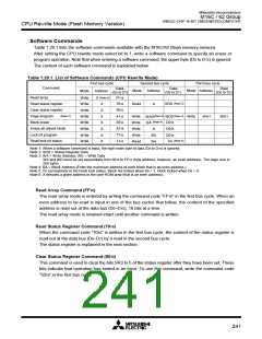
Table 1.29.1. List of Software Commands (CPU Rewrite Mode)
First bus cycle
Second bus cycle
Third bus cycle
Command
Data
(D to D
Data
to D
Data
to D7)
Mode Address
Mode Address
Mode
Address
0
7)
(D
0
7
)
(D
0
(Note 6)
Read array
Write
Write
Write
Write
Write
Write
Write
Write
X
FF16
7016
5016
4116
2016
A716
7716
7116
Read status register
Clear status register
X
X
X
X
X
X
X
Read
X
SRD (Note 2)
(Note 3)
(Note 3)
WA0(Note 3)
Page program
WD0
Write
WA1
WD1
Write
Write
Write
Write
Read
BA (Note 4)
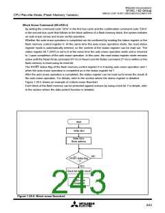
Block erase
D016
D016
Erase all unlock block
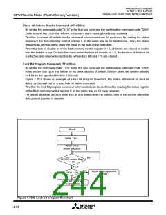
Lock bit program
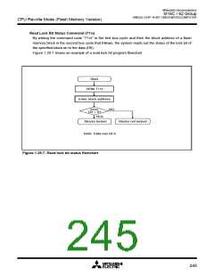
Read lock bit status
X
BA
BA
D016
(Note 5)
6
D
Note 1: When a software command is input, the high-order byte of data (D
Note 2: SRD = Status Register Data
8 to D15) is ignored.
Note 3: WA = Write Address, WD = Write Data
WA and WD must be set sequentially from 0016 to FE16 (byte address; however, an even address). The page size is
256 bytes.
Note 4: BA = Block Address (Enter the maximum address of each block that is an even address.)
Note 5: D6 corresponds to the block lock status. Block not locked when D6 = 1, block locked when D6 = 0.
Note 6: X denotes a given address in the user ROM area (that is an even address).
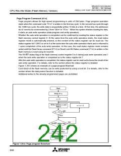
Read Array Command (FF16)
The read array mode is entered by writing the command code “FF16” in the first bus cycle. When an
even address to be read is input in one of the bus cycles that follow, the content of the specified
address is read out at the data bus (D0–D15), 16 bits at a time.
The read array mode is retained intact until another command is written.
Read Status Register Command (7016)
When the command code “7016” is written in the first bus cycle, the content of the status register is
read out at the data bus (D0–D7) by a read in the second bus cycle.
The status register is explained in the next section.
Clear Status Register Command (5016)
This command is used to clear the bits SR3 to 5 of the status register after they have been set. These
bits indicate that operation has ended in an error. To use this command, write the command code
“5016” in the first bus cycle.
241

 MITSUBISHI [ Mitsubishi Group ]