Mitsubishi microcomputers
M16C / 62 Group
SINGLE-CHIP 16-BIT CMOS MICROCOMPUTER
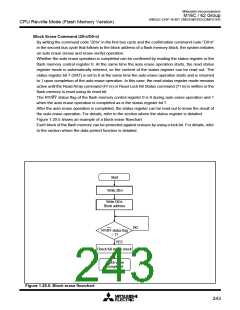
CPU Rewrite Mode (Flash Memory Version)
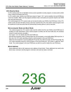
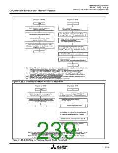
Program in ROM
Start
Program in RAM
*1
Single-chip mode, memory expansion
mode, or boot mode
(Boot mode only)
Set user ROM area select bit to “1”
Set CPU rewrite mode select bit to “1” (by
writing “0” and then “1” in succession)(Note 2)
Set processor mode register (Note 1)
Transfer CPU rewrite mode control
program to internal RAM
Using software command execute erase,
program, or other operation
(Set lock bit disable bit as required)
Jump to transferred control program in RAM
(Subsequent operations are executed by control
program in this RAM)
Execute read array command or reset flash
memory by setting flash memory reset bit (by
writing “1” and then “0” in succession) (Note 3)
*1
Write “0” to CPU rewrite mode select bit
(Boot mode only)
Write “0” to user ROM area select bit (Note 4)
End
Note 1: During CPU rewrite mode, set the main clock frequency as shown below using the main clock divide ratio
select bit (bit 6 at address 000616 and bits 6 and 7 at address 000716):
6.25 MHz or less when wait bit (bit 7 at address 000516) = “0” (without internal access wait state)
12.5 MHz or less when wait bit (bit 7 at address 000516) = “1” (with internal access wait state)
Note 2: For CPU rewrite mode select bit to be set to “1”, the user needs to write a “0” and then a “1” to it in
succession. When it is not this procedure, it is not enacted in “1”. This is necessary to ensure that no
interrupt or DMA transfer will be executed during the interval.
Note 3: Before exiting the CPU rewrite mode after completing erase or program operation, always be sure to
execute a read array command or reset the flash memory.
Note 4: “1” can be set. However, when this bit is “1”, user ROM area is accessed.
Figure 1.29.2. CPU Rewrite Mode Set/Reset Flowchart
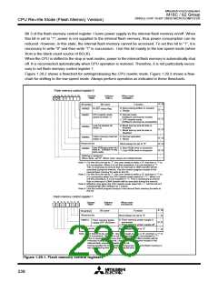
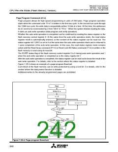
Program in ROM
Program in RAM
*1
Start
Transfer the program to be executed in the
low speed mode, to the internal RAM.
Set flash memory power supply-OFF bit to “1”
(by writing “0” and then “1” in succession)(Note 1)
Jump to transferred control program in RAM
(Subsequent operations are executed by control
program in this RAM)
Switch the count source of BCLK.
X
IN stop. (Note 2)
Process of low speed mode
*1
X
IN oscillating
Wait until the XIN has stabilized
Switch the count source of BCLK (Note 2)
Set flash memory power supply-OFF bit to “0”
Wait time until the internal circuit stabilizes
(Set NOP instruction about twice)
End
Note 1: For flash memory power supply-OFF bit to be set to “1”, the user needs to write a “0” and then a “1” to it in
succession. When it is not this procedure, it is not enacted in “1”. This is necessary to ensure that no
interrupt or DMA transfer will be executed during the interval.
Note 2: Before the count source for BCLK can be changed from XIN to XCIN or vice versa, the clock to which
the count source is going to be switched must be oscillating stably.
Figure 1.29.3. Shifting to The Low Speed Mode Flowchart
239

 MITSUBISHI [ Mitsubishi Group ]